
BD8174MUV IC Overview and Pinout
Explore the BD8174MUV IC Step-Up DC-DC Guide, your complete reference for this IC’s startup sequence, detailed block diagram, pin descriptions, and parts list. This guide provides step-by-step insights into how the IC operates within TFT panels, with clear images illustrating the startup sequence and internal block functionality, making it an essential resource for technicians, engineers, and students working on DC-DC converter circuits.
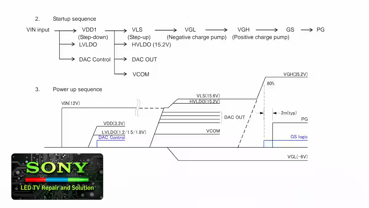
BD8174MUV IC Startup Sequence
The image below illustrates the complete BD8174MUV IC startup sequence, showing step-by-step how the IC powers up and how the various voltages and signals are activated in order. This visual guide provides a clear understanding of the startup behavior, helping technicians and students alike to analyze the IC’s operation within TFT panels. By following this sequence, you can better diagnose issues, understand signal flow, and ensure proper integration of the IC in your DC-DC converter circuits.
BD8174MUV IC Typical Application Circuit
The image below shows a typical application circuit for the BD8174MUV IC Step-Up DC-DC Guide, illustrating how the IC and associated components are connected in a real-world setup. This visual reference helps technicians and students understand the practical integration of the IC, including the placement of passive and active components, signal paths, and voltage flow. By studying this circuit, you can confidently design, troubleshoot, and implement the IC in TFT panel power supply applications.

BD8174MUV IC Block Diagram
The image below illustrates the internal block diagram of the BD8174MUV IC, showing all key functional blocks along with their voltage inputs and outputs. Each output voltage, including VGL, VGH, and other critical signals, is clearly represented to provide a complete understanding of how the IC manages step-up DC-DC conversion within TFT panels. This detailed visual guide allows technicians and students to analyze voltage distribution, signal flow, and internal operation, making it easier to troubleshoot and integrate the IC into practical circuits.

BD8174MUV IC Pin Description
1 PVCC1 Boost DC/DC load switch input. See Boost DC/DC (1) for more information.
2 PVCC1 Boost DC/DC load switch input. See Boost DC/DC (1) for more information.
3 CPPCTL Positive charge pump control input. See charge pump (4) for more information.
4 HVCC Power supply pin for charge pump, buffer amplifier and HV_LDO.
5 VGL_S Negative charge pump output VGL feedback input.
6 CPN Negative charge pump regulator driver output. Drive pin for negative charge pump.
See charge pump (4) for more information.
7 CPP1 Positive charge pump regulator driver output1. Drive pin for positive charge pump.
See charge pump (4) for more information.
8 CPP2 Positive charge pump regulator driver output2. Drive pin for positive charge pump.
See charge pump (4) for more information.
9 CPGND Power grounding pin at charge pump.
10 CPD2 Positive charge pump internal switching diode output2.
11 CPD1 Positive charge pump internal switching diode output1.
12 VGH Positive charge pump output VGH. Connect output capacitor from this pin to GND.
13 COM Gate shading output pin.
14 DRN Termination of the low side switch of the gate voltage shading block.
15 CTL Gate shading control input pin.
16 THR Gate shading Low level setting pin.
17 VCOM VCOM Output
18 INN VCOM input-.
19 INP VCOM input+.
20 HVLDO HV_LDO output pin. Insert output capacitance for GND.
21 FBLD1 HV_LDO feedback input pin.
22 DACGND GND pin for DAC.
23 SCP Short protection delay
24 OUT0 Gamma output pin.
25 OUT1 Gamma output pin.
26 OUT2 Gamma output pin.
27 OUT3 Gamma output pin.
28 GND Grounding pin.
29 SDA Serial data input pin.
30 SCL Serial clock input pin.
31 LVLDO LV_LDO output pin. Output outputs 1.8V/ 1.5V/ 1.2V (typ). Insert output capacitance for GND.
32 REG5 Internal power supply 5.0V output pin. Connect 0.1µF from this pin to ground.
33 VDD_S Buck DC/DC output VDD feedback input. No external registance necessary for feedback register.
34 GCTL Boost DC/DC load switch PGATE control input. For details, refer to information in Boost DC/DC (1).
35 SW2 Buck DC/DC switching output. Due to reduce EMI, make a wiring thick and short.
36 PGND2 Buck DC/DC switching node power grounding pin. Due to reduce EMI, make a wiring thick and short.
37 BOOT Buck DC/DC bootstrap pin. This pin generates the gate drive voltage for the Buck converter.
Connect 0.1µF from this pin to the switch pin of step down converter, SW2.
38 LVCTL LVLDO output voltage setting pin.
39 PG Power good output. After positive charge pump output VGH startup, It will be ON. For Buck DC/DC output,
Pull-UP and use it. If you don’t use it, It will open.
40 PVCC2 Buck DC/DC high side MOSFET power supply input. Connect a capacitor as close to PVCC pin as Possiple.
BD8174MUV IC Parts List
Below is the complete BD8174MUV IC Step-Up DC-DC Guide parts list, showing all components used with this IC. This detailed reference helps technicians and students identify each part and understand how they integrate with the IC for proper circuit operation.

Conclusion
In conclusion, the BD8174MUV IC Step-Up DC-DC Guide provides a complete technical reference for anyone working with this IC. From the startup sequence and block diagram to detailed pin descriptions and parts list, this guide equips technicians, engineers, and students with the knowledge needed to understand, troubleshoot, and effectively implement the IC in TFT panel circuits. With these insights, you can ensure accurate voltage management, signal integrity, and optimal performance in your projects.
BD9397EFV Backlight Driver Guide

Shaukat Ali has over 30 years of experience in LED TV repair, specializing in chip-level repair work. He is an expert in Sony LED TVs, and also repairs other major brands like Samsung, TCL, Orient, and Haier. His expertise includes display panel faults, motherboard issues, power supply circuits, T-Con, and HDMI faults. Based in Lahore, he shares real-time fault finding cases from daily repair work to help technicians and learners with practical experience.
📞 Contact: +92 321 4066054