
MT4761B01-1 Complete Test Point & Panel Reference
Have you ever wondered where the real reference data comes from when dealing with different faults in an LCD panel? This is exactly what the 8656-JC513 COF & Scalar Data Guide is designed for, specifically related to the MT4761B01-1 panel used in this setup. This guide provides complete Chip On Film (COF) reference information along with scalar connection details that are essential for proper panel-level understanding. It also includes reference images that make fault identification and testing much easier in real repair situations. This content is especially helpful for beginners as well as professional technicians who work on LCD panel troubleshooting, testing, and board-level diagnosis, allowing them to clearly understand COF behavior and related test points in a practical and technical way.
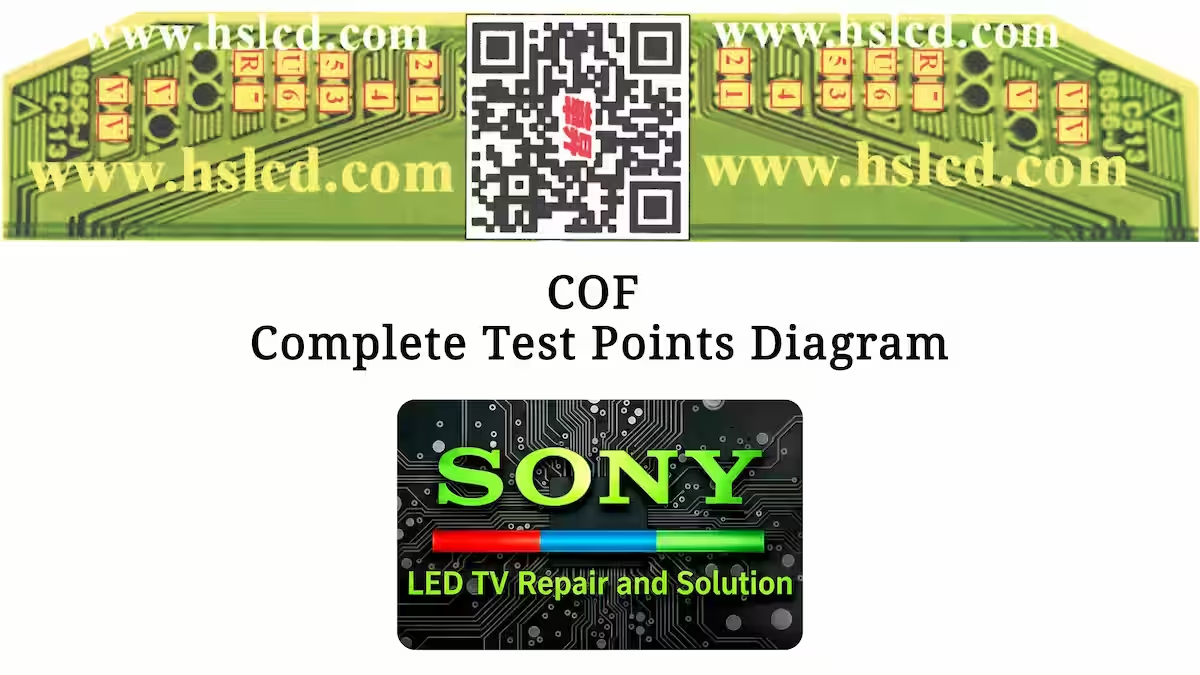
COF Complete Test Points Diagram
The image below shows the complete Chip On Film (COF) reference for 8656-JC513, where all test points are clearly marked and visible for proper understanding. Through this diagram, a technician can easily identify each COF test point and understand how signals are distributed across the panel structure. It is very helpful during real troubleshooting cases such as line faults, display issues, or signal loss at board level. This visual reference allows accurate analysis of the COF behavior and makes testing much easier and more reliable during repair work.
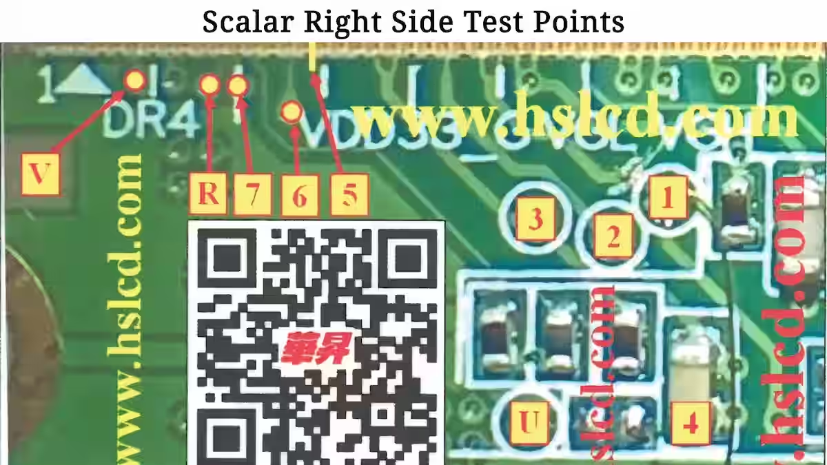
Scalar Right Side Test Points
The image below shows the right side scalar section of the MT4761B01-1 panel, where all key test points and signal paths are clearly visible. This section is very important for understanding how the scalar board distributes signals towards the display processing stage. A technician can easily trace voltage lines, data signals, and check connectivity issues from this side during fault diagnosis. It helps in identifying problems like display distortion, signal loss, or communication errors between the main board and panel.
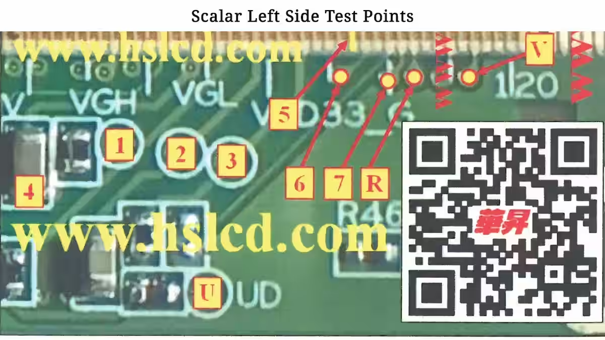
Scalar Left Side Test Points
The image below represents the left side scalar section of the MT4761B01-1 panel, showing detailed test points and signal routing paths. This section plays a key role in balancing and processing display signals across the panel structure. Technicians can use this reference to check continuity, voltage levels, and signal behavior during repair work. It is especially useful for diagnosing issues related to partial display, vertical lines, or scalar communication faults.
COF Function in Panel Structure
The Chip On Film (COF) in an LCD panel plays a key role in the overall structure, especially in signal and voltage distribution. In the MT4761B01-1 panel, it controls pixel rows and manages display data between the panel glass and main processing section. It also ensures proper signal timing and helps distribute required voltages for stable panel operation. Understanding this section is very important for both beginners and technicians, as many display faults are directly linked with COF behavior.
COF Pin Test Point Description
- Pin 1 (VGH +25.8V) is a high positive gate voltage used in the COF circuit to drive the TFT switches inside the panel. It helps in turning on the pixels properly during scanning. If this voltage drops or becomes unstable, the display may show issues like vertical lines, dim picture, or complete loss of image.
- Pin 2 (VGL -5.8V) is the negative gate voltage used in the COF circuit to properly turn off the TFT switches inside the panel. It works opposite to VGH and is essential for correct pixel control during scanning. If this voltage is missing, low, or unstable, it can cause display issues like flickering, distorted image, or vertical line problems on the screen.
- Pin 3 (VDD 3.3V) is the main logic supply voltage for the COF circuit. It powers the internal control IC and supports data processing inside the panel. If this voltage is low, unstable, or missing, the panel may show no display, random operation, or complete failure to start the image signal properly.
- Pin 4 (GND) is the ground reference point of the COF circuit. It completes the electrical circuit and provides a stable reference for all voltage levels in the panel. If this ground connection becomes weak or open, it can cause unstable operation, signal disturbance, or abnormal display behavior such as flickering or no display.
- Pin 5 (STV 0.05V) is the start vertical signal line used in the COF circuit to control the vertical scanning sequence of the panel. It works as a timing reference for shifting data across pixel rows. If this signal is weak, missing, or unstable, it can result in vertical line defects, frame freezing, or improper screen scanning behavior.
- Pin 6 (CKV +2.62V) is the clock vertical signal used in the COF circuit to synchronize the vertical scanning process of the panel. It works as a timing pulse that controls the sequential driving of pixel rows. If this voltage is missing, weak, or unstable, it can cause display issues like vertical lines, unstable image, or improper frame shifting on the screen.
- Pin 7 (OE +2.62V) is the Output Enable signal used in the COF circuit to control when the panel data output is active or disabled. It plays an important role in managing proper signal timing during display operation. If this voltage is missing or unstable, the panel may show no display, random flickering, or improper image activation issues.
- Pin U (UD +3.3V) is the logic control supply line in the COF circuit that supports internal data processing and signal handling functions. It ensures stable operation of the control section inside the panel. If this voltage is low, missing, or unstable, the panel may show no display, distorted image, or random signal behavior on the screen.
- Pin R (STVR 0.06V) is a vertical start reference signal used in the COF circuit to control and synchronize the right-side scanning process of the panel. It helps in proper timing of pixel row activation on the display. If this signal is weak, missing, or unstable, it can result in vertical line issues, partial display, or improper screen scanning behavior on the right side of the panel.
- Pin V (V-VCOM +6.9V) is the common voltage reference used in the COF circuit for proper pixel alignment and display stability. It plays a key role in balancing the liquid crystal operation inside the panel. If this voltage is incorrect, unstable, or missing, the screen may show flickering, uneven brightness, or image distortion issues across the display.
Conclusion
This 8656-JC513 COF & Scalar Data Guide for the MT4761B01-1 panel gives a complete technical reference of COF structure, scalar test points, and voltage behavior. From VGH, VGL, VDD, STV, CKV, OE, UD to VCOM, every pin plays a critical role in proper panel operation and signal distribution. Understanding these points helps in accurate fault diagnosis, especially in cases of line issues, display distortion, or complete no display problems.
For technicians working on the MT4761B01-1 panel, this guide is a useful reference during real repair work. Any disturbance in COF voltages or signal lines can directly affect the screen performance, so proper testing and analysis of each pin is very important. By using this COF data structure and scalar reference, troubleshooting becomes more systematic and reliable for both beginners and experienced technicians.
Related Articles
If you want to read more technical articles on Chip On Film (COF) and panel-level troubleshooting, you can find the related guides below. These articles will help you understand different COF faults, test points, and real repair solutions in more detail. All links are available below for further reading and learning.
8656-FCYOB –Read More
NT61303H-C52A2B –Read More

Shaukat Ali has over 30 years of experience in LED TV repair, specializing in chip-level repair work. He is an expert in Sony LED TVs, and also repairs other major brands like Samsung, TCL, Orient, and Haier. His expertise includes display panel faults, motherboard issues, power supply circuits, T-Con, and HDMI faults. Based in Lahore, he shares real-time fault finding cases from daily repair work to help technicians and learners with practical experience.
📞 Contact: +92 321 4066054