
Complete Test Points panel with V320BJ2-XCO1
The NT39530H-C5203 Side COF Test Points guide for the V320BJ2-XCO1 panel provides detailed COF references along with practical test point information for repair work. In this article, the scaler strip layout, important voltage lines, and complete testing points are explained in a clear and technician-friendly format. The purpose of this visual reference is to make panel signal tracing and fault diagnosis easier, helping technicians perform accurate checking and faster troubleshooting during repair process.
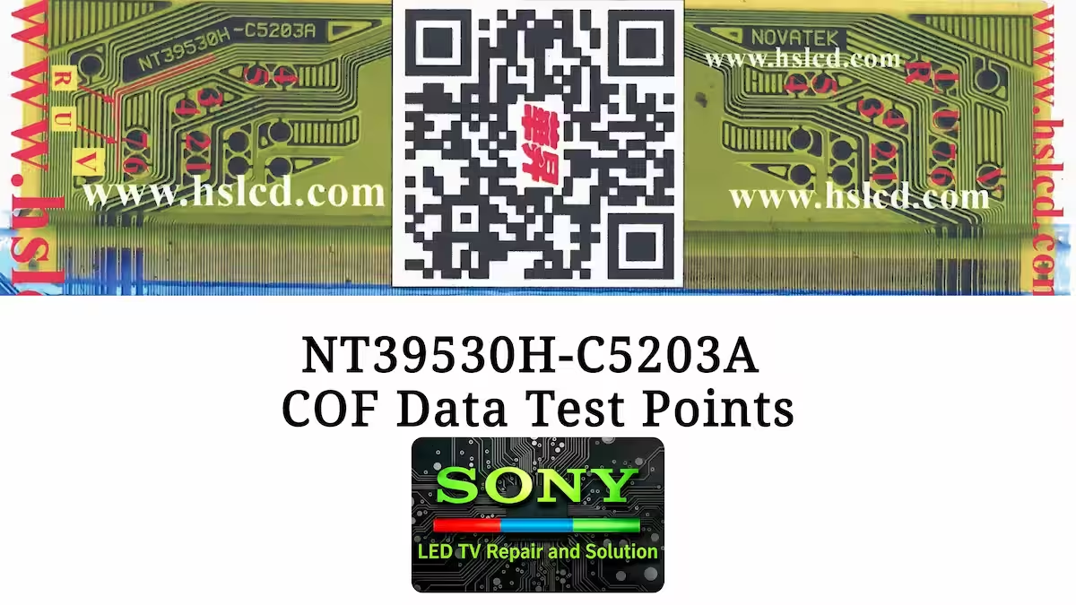
NT39530H-C5203 Gate COF Data Sheet
The image below shows the complete gate COF test points of the V320BJ2-XCO1 panel with important voltage and signal reference details for practical troubleshooting. This visual reference helps in understanding the COF layout, signal routing, and panel driving structure more clearly during repair work. All major testing points are marked for easier diagnosis, while the scaler strip references for both left and right sides are also included below to provide a better overall understanding of the panel section.
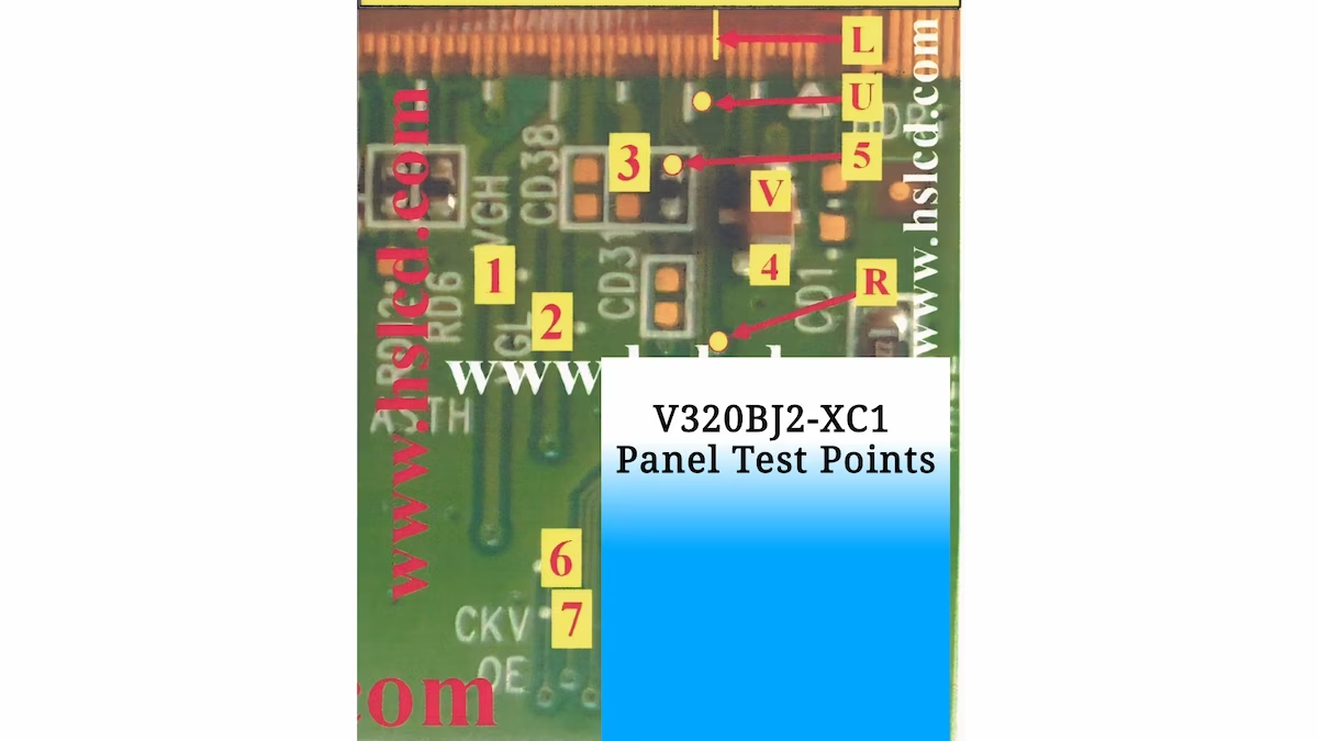
V320BJ2-XCO1 Scaler Test Points
The image below shows the complete scaler strip test points and signal lines of the V320BJ2-XCO1 panel with clearly marked references for practical troubleshooting. This section includes important voltage points, signal paths, and connection details that help technicians understand the panel driving circuit more accurately during repair work. Using this visual reference makes signal tracing and fault diagnosis easier while working on panel-related issues.
NT39530H-C5203 Gate COF Overview
Gate COF is an important section of the TFT panel driving system that controls the scanning process of the display line by line. It works with voltages like VGH and VGL to switch TFT cells properly during image generation. This section plays a major role in stable panel operation and clear picture output. If any fault develops in the gate COF area, the panel may show display issues such as vertical lines, no display, or improper scanning on the screen.
Technical Experience Note
This COF data is shared as a practical reference guide for panel repair work. During bypass repair, always handle the panel carefully, especially when dealing with VGH and VGL short lines. In many cases, proper isolation requires cutting from both the glass side and the COF side to fully remove the internal short condition. After isolation, using jumper wire bypass is usually a more stable and reliable solution for long-term panel performance.
COF DATA and scalar test points
- VGH-20.28+V
- VGL-5.8-V
- VDD-3.3+V
- GND 0V
- STV-IN-0.002+V
- CKV-1,7+V
- OE-1.0+V
- U-UD-3.3+V
- L L/R-3.3+V
- R-STVR-0.03+V
- V-V-COM-7.3+V
Conclusion
In conclusion, this NT39530H-C5203 Side COF Test Points for the PT320AT01-1-XC C2 panel provides a clear and practical reference for understanding COF structure, scaler test points, and key pin voltage details. It is very useful for technicians during real repair work, especially for accurate fault finding and signal tracing on panel-level issues. With proper application of this data, COF diagnosis becomes more efficient, reliable, and easier during display and panel troubleshooting tasks.
Related Articles
If you want to read more chip-on-film data and panel repair articles, you can check the links below. We have shared practical guides for different COF models and panel types for better understanding and troubleshooting. Keep learning and improving your repair skills.
8656-JC513 COF & Scalar Data Guide – Read More
Download the complete PDF file here.
NT39525h-c5602b Complete COF Data Analysis
Sony KD-55X9000A Red Light Blinking Fix

Shaukat Ali has over 30 years of experience in LED TV repair, specializing in chip-level repair work. He is an expert in Sony LED TVs, and also repairs other major brands like Samsung, TCL, Orient, and Haier. His expertise includes display panel faults, motherboard issues, power supply circuits, T-Con, and HDMI faults. Based in Lahore, he shares real-time fault finding cases from daily repair work to help technicians and learners with practical experience.
📞 Contact: +92 321 4066054