
Complete COF data with scalar strip test points
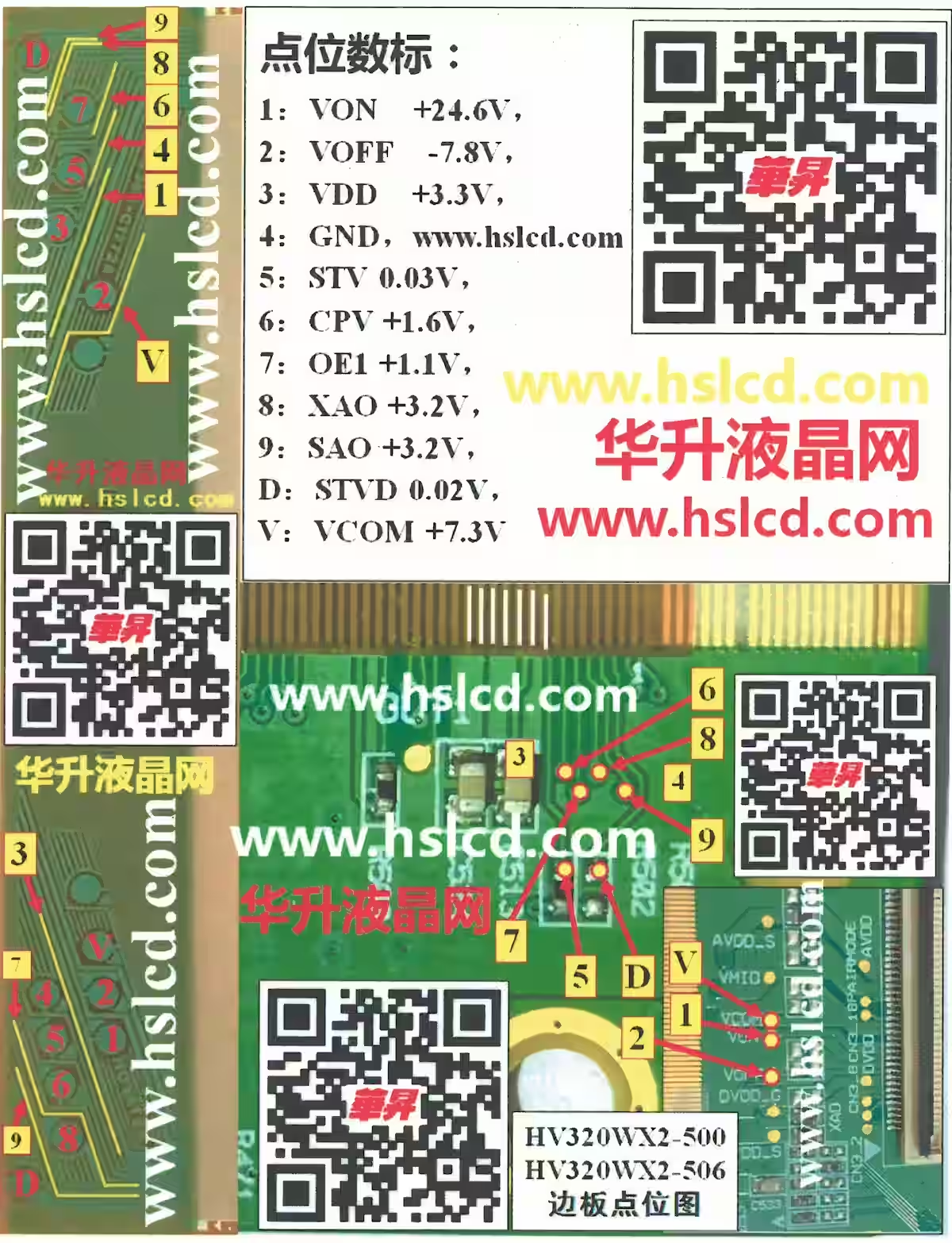
NT39538H-C1272A COF DATA with complete test point details of scaler panels HV230WX2-500 and HV320WX2-506 is provided in this article along with a full PDF preview for practical reference. If you are working on panel-level faults such as display lines, no display, half screen, or signal issues, this COF data can help you understand the scaler connections and important test points more clearly.
In this guide, you will find structured COF information prepared especially for technicians who need accurate panel data during fault finding. Our purpose is to make troubleshooting easier by sharing verified and organized COF details that can save time during practical repair work. This is a complete and professional COF data guide published for the support of technicians working on Sony LED TV panels.

NT39538H COF Voltage Guide
1 VON (+24.6V) is the positive gate-on voltage supplied to the panel driver section through the COF. This voltage plays a critical role in activating the TFT gates during display operation. When VON is present at the correct level, the panel is able to drive pixels properly and produce a stable picture.
In normal working condition, this voltage should remain stable around +24.6V. If VON is missing, low, or fluctuating, the panel may show symptoms such as no display, dim screen, vertical lines, or incomplete image formation.
While testing, measure this voltage carefully using a digital multimeter with proper ground reference. If the voltage is absent, check the VGH generation circuit, DC-DC section, or related boosting components on the panel board. Any abnormality in this line directly affects panel gate driving performance.
2 VOFF (-7.8V) is the negative gate-off voltage used in the TFT panel driving circuit. This voltage is responsible for turning the pixel transistors completely off during scanning operation. Without a proper VOFF level, the panel cannot control the pixel switching accurately.
In normal working condition, VOFF should remain stable around -7.8V. If this voltage becomes weak, missing, or unstable, common symptoms may include faded display, ghosting effect, vertical shadow lines, or image retention issues.
During testing, always confirm the negative polarity carefully while measuring with a digital multimeter. If VOFF is not present, inspect the negative voltage generation section, charge pump circuit, or related filtering components on the panel board. An imbalance between VON and VOFF directly affects the gate control timing and overall display quality.
3 VDD (+3.3V) is the main logic supply voltage for the COF and scaler interface section. This voltage powers the internal control circuitry responsible for signal processing and communication between the panel and the main board. Without a stable VDD supply, the COF cannot operate correctly.
Under normal conditions, VDD should measure close to +3.3V and remain steady. If this voltage is low, missing, or fluctuating, the panel may show symptoms such as no display, distorted image, unstable picture, or complete panel inactivity.
When testing, measure the voltage carefully with proper ground reference. If VDD is not stable, inspect the regulator section, related LDO IC, filtering capacitors, or supply line from the main board. Even a slight drop in this voltage can disturb the digital signal processing and affect overall panel performance.
4 GND (Ground) is the reference line for all voltages present on the COF and panel circuit. Every voltage measurement including VON, VOFF, and VDD is taken with respect to this ground point. A stable and proper ground connection is essential for accurate signal transmission and voltage regulation.
In normal condition, GND should show zero potential difference when measured against chassis or panel ground. If the ground line is open, weak, or has high resistance, it can cause unstable voltages, flickering display, random lines, or complete panel malfunction.
5 STV (+0.03V) stands for Start Vertical signal, which is responsible for initiating the vertical scanning sequence in the panel driver circuit. This signal works in coordination with the gate driver section to control the timing of vertical line activation across the display.
In standby measurement using a digital multimeter, STV may show a very low DC value such as +0.03V because it is actually a pulse signal rather than a fixed voltage line. During active operation, this line carries timing pulses that cannot be fully analyzed with a standard multimeter and may require an oscilloscope for accurate waveform observation.
If the STV signal is missing or not functioning properly, the panel may show symptoms like no display, vertical freeze, half screen issue, or improper line scanning. When troubleshooting, always verify the signal path from the scaler to the COF input and check for any open track or shorted component affecting the timing line.
While testing, always confirm that your multimeter’s negative probe is connected to a reliable ground point. Poor grounding can lead to incorrect readings and misdiagnosis during fault finding. In many cases, grounding issues are overlooked, but they directly affect overall panel stability and signal integrity.
6 CP (+1.6V) generally refers to the Clock Pulse line used in the panel driving circuit. This signal plays an important role in synchronizing data transfer between the scaler and the COF driver section. It ensures that pixel data is shifted and processed in proper timing sequence.
When measured with a digital multimeter, CP may show a DC level around +1.6V because it is a pulse-based signal. In actual operation, this line carries clock pulses that control data shifting inside the driver IC. For accurate signal verification, an oscilloscope is recommended to observe the waveform and pulse consistency.
If the CP signal is weak, missing, or unstable, the display may show symptoms such as vertical lines, distorted image, frozen screen, or no picture at all. During fault finding, inspect the clock generation section, signal tracks, and related components between the scaler output and COF input. Any interruption in this line can disturb the entire panel data timing system.
7 OE1 (+1.1V) stands for Output Enable 1, a control signal used in the COF driver to manage the enabling of pixel output for a specific section of the panel. This signal ensures that only the intended pixels are activated during the scanning sequence, preventing display artifacts or overlapping lines.
When measured with a digital multimeter, OE1 may show around +1.1V DC, though in operation it actually functions as a pulse or logic signal. Accurate timing and waveform inspection using an oscilloscope can provide deeper verification of its proper operation.
If OE1 is missing, weak, or unstable, the panel may exhibit symptoms such as partial display, flickering, missing lines, or ghosting effects. While troubleshooting, always check the signal path from the scaler to the COF driver and inspect related components like resistors, capacitors, and traces. Proper OE1 operation is crucial for stable pixel control and overall display quality.
8 XAO (+3.3V) is the analog output supply voltage for specific driver circuits within the COF. This voltage powers internal analog sections that handle signal amplification and precise pixel driving, ensuring smooth grayscale and color reproduction on the panel.
In normal conditions, XAO should measure stable around +3.3V. Any drop, fluctuation, or absence of this voltage can result in issues such as faded colors, uneven brightness, or distorted images. Since XAO feeds analog circuits, stability is critical for maintaining uniform display performance across the panel.
During testing, always measure this voltage with respect to GND. If XAO is abnormal, inspect the voltage regulator, filtering capacitors, or analog driver IC components. Ensuring a stable XAO supply is essential for proper analog signal processing and high-quality display output.
D STVD (+0.02V) stands for Start Horizontal/Vertical Display signal, which is used to initiate the vertical data scanning process in the panel driver circuit. This line works together with the gate driver and clock signals to ensure that each row of pixels is activated in the correct timing sequence.
When measured with a digital multimeter, STVD may show a very low DC value like +0.02V because it carries pulse signals rather than a fixed voltage. For accurate analysis of this timing signal, an oscilloscope is recommended to observe pulse width, frequency, and stability.
If STVD is missing, unstable, or delayed, common panel issues may include vertical freeze, no display, partial image, or misaligned lines. During troubleshooting, inspect the signal path from the scaler IC to the COF input, along with any resistors, capacitors, or traces that could affect the timing line. Proper STVD operation is critical for correct vertical scanning and stable panel performance.
V VCOM (+7.3V) is the common voltage reference for the LCD panel, applied to the liquid crystal layer to stabilize the pixel voltage swings. This voltage ensures uniform brightness and contrast across the display and prevents flickering or image instability.
Under normal conditions, VCOM should remain stable at approximately +7.3V. Any fluctuation, absence, or deviation can lead to visible issues such as uneven brightness, ghosting, flickering, or washed-out images. Since VCOM directly affects all pixels simultaneously, stability in this line is critical for maintaining consistent image quality.
When testing, measure VCOM with respect to GND using a reliable multimeter. If the voltage is abnormal, inspect the VCOM generation circuit, including buffers, resistors, and capacitors on the COF or panel board. Ensuring a proper VCOM is key for smooth grayscale performance and overall display reliability.
NT39538H COF Layout with Test Points
The image below shows the complete NT39538H COF layout with all test points for the COF and scaler connections of the panel. This reference provides a clear view of the chip-on-film structure, helping technicians accurately identify and measure each test point during troubleshooting. It serves as an essential visual guide for precise panel-level repair and fault diagnosis.
Complete PDF Preview File Zoom and Scroll
Conclusion
In conclusion, NT39538H-C1272A COF DATA provides a complete reference for all test points, scaler connections, and chip-on-film layout details for Sony LED TV panels. By using this guide, technicians can efficiently perform panel-level troubleshooting, verify voltages, and ensure accurate fault diagnosis. Having access to such detailed COF data saves time, reduces errors, and strengthens practical repair skills for every professional working with these panels.
NT39538H-C1260A COF Test Points & Voltage Analysis
V320BJ2-XC01 Side COF Details and Voltage Analysis
Sony LED TV Red Light Blink Error Codes

Shaukat Ali has over 30 years of experience in LED TV repair, specializing in chip-level repair work. He is an expert in Sony LED TVs, and also repairs other major brands like Samsung, TCL, Orient, and Haier. His expertise includes display panel faults, motherboard issues, power supply circuits, T-Con, and HDMI faults. Based in Lahore, he shares real-time fault finding cases from daily repair work to help technicians and learners with practical experience.
📞 Contact: +92 321 4066054