
Complete Test Points with V500Hj1-PE8 C3
Explore the complete NT39565H-C5253B COF DATA with test points for the V500DK1 panel, where you can find detailed COF information and accurate test point references for practical use. This guide includes scaler strip details, complete test point layout, and essential voltage information to help understand panel behavior clearly. All connections and signal paths are explained in a simple and technician-friendly way, making it easier to perform fast and accurate fault finding during repair work.
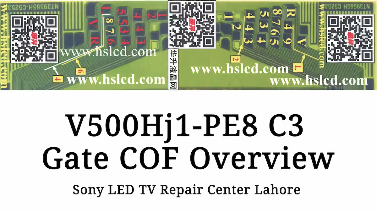
NT39565H-C5253B Gate COF Data Sheet
In the image below, you can see the gate COF test points of the V500Hj1-PE8 C3 panel in complete detail, including all important voltage and signal reference points for practical use. This image provides a clear view of the COF structure and its connections, making it easier to understand the panel’s driving behavior during repair work. The scaler strip images for both left and right sides are also shared below for further reference and complete panel understanding.
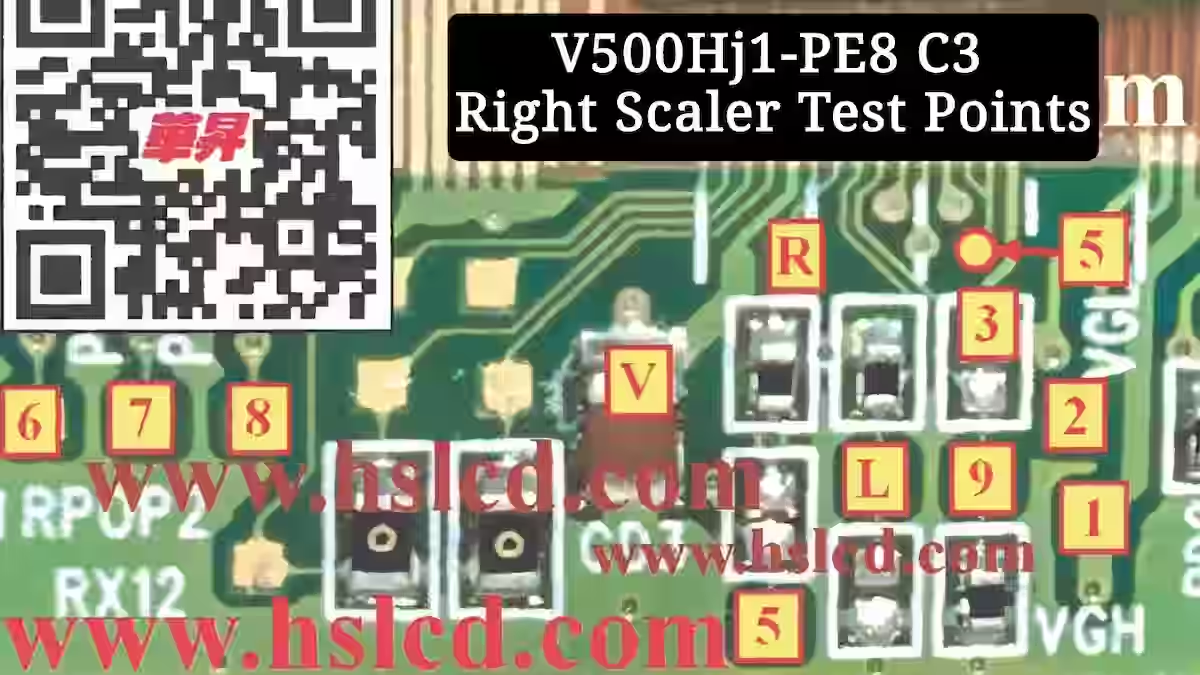
V500Hj1-PE8 C3 Right Scaler Test Points
In the image below, you can see all the test points and signal lines of the right-side scaler strip of the V500DK1 panel clearly marked for practical reference. This section includes important voltage points and signal paths that help in understanding the panel’s right-side driving behavior. By using this image, technicians can easily trace connections and perform accurate fault finding during repair work.
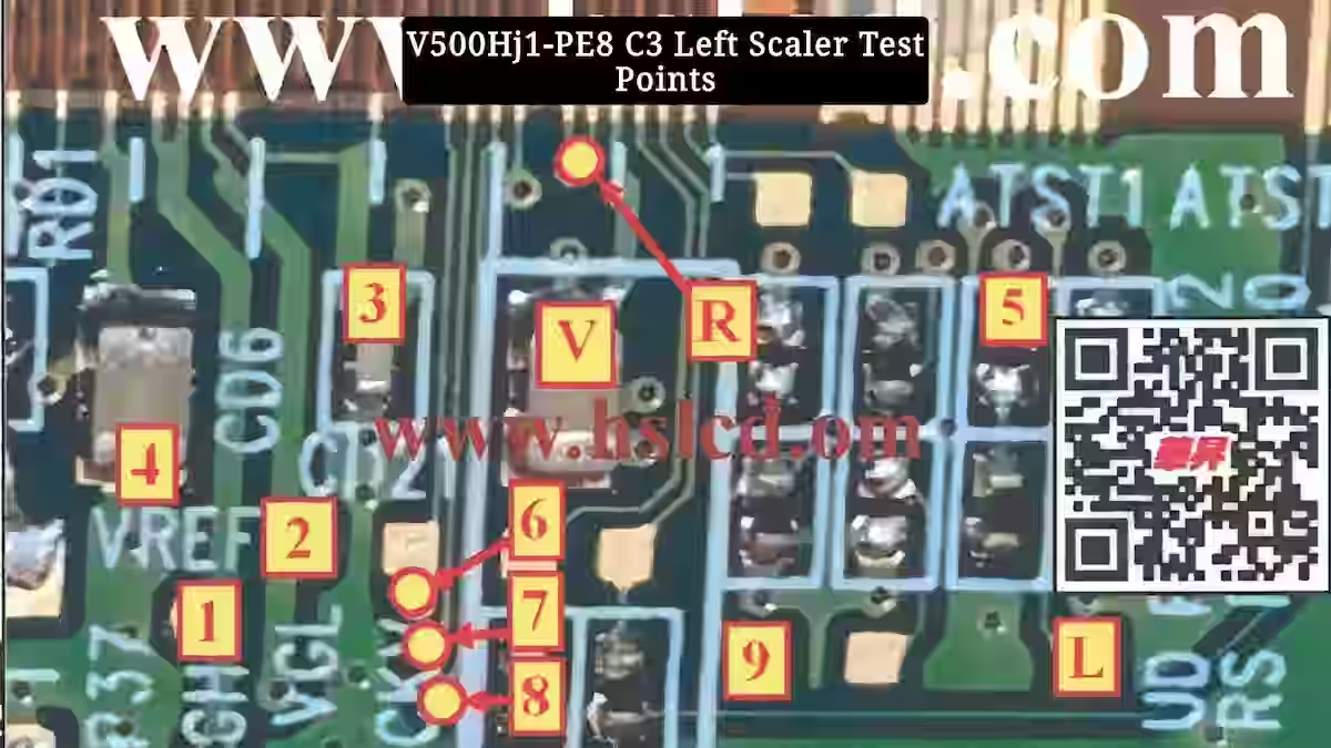
V500Hj1-PE8 C3 Left Scaler Test Points
In the image below, you can see all the test points and signal lines of the left-side scaler strip of the V500DK1 panel clearly marked for practical reference. This section includes important voltage points and signal paths that help in understanding the panel’s left-side driving behavior. By using this image, technicians can easily trace connections and perform accurate fault finding during repair work.
V500Hj1-PE8 C3 Gate COF Overview
Gate COF is a key section of the TFT panel driving system that controls the row-by-row scanning of the display. It generates and distributes gate signals in a proper sequence so each line of pixels can be activated accurately during image formation. This section works closely with driving voltages like VGH and VGL to ensure correct ON and OFF switching of TFT cells. In simple terms, Gate COF manages the vertical scanning process of the panel and plays an important role in stable and clear picture output. If there is any issue in this area, the panel may show no display, vertical lines, or improper scanning behavior on the screen.
NT39565H-C5253B COF Pin Description
- Pin 1 VGH +27.6V
This voltage is used for the gate high driving section of the TFT panel and is responsible for turning the pixel lines ON during scanning. It provides the required high-level switching signal to the gate driver IC for proper row activation. If this voltage is missing or low, the panel may show no display, blank screen, or complete failure in image formation.
- Pin 2 VGL -7.8V
This voltage is used for the gate low driving section of the TFT panel and works opposite to VGH. It helps in properly turning the pixel lines OFF during scanning by providing negative switching voltage to the gate driver IC. If this voltage is missing or unstable, the panel may show flickering, distorted image, or improper line scanning on the display.
- Pin 3 VDD +3.3V
This is the main logic supply voltage for the panel control and timing circuits. It powers the internal processing system that manages signal timing and data distribution across the display. If this voltage is missing or low, the panel may remain dead, fail to start, or show no display on the screen.
- Pin 4 GND
This is the main ground reference point of the panel circuit and completes the return path for all operating voltages. It provides stable reference for VGH, VGL, VDD, and all signal lines to work properly. If this ground connection is weak or open, the panel may show unstable display, flickering, or complete no operation.
- Pin 5 STV 0.04V
This is the vertical start pulse signal used for initiating frame scanning in the TFT panel. It controls the timing sequence that starts row-by-row display activation in the correct order. If this signal is missing or unstable, the panel may show no display, broken scanning, or vertical line distortion on the screen.
- Pin 6 CKV +1.71V
This is the clock pulse signal used for vertical scanning control in the TFT panel. It provides timing pulses to the gate driver IC, which helps in shifting and activating each row step by step during display operation. If this voltage is missing or unstable, the panel may show flickering, improper scanning, or no display on the screen.
- Pin 7 OE2 +1.36V
This is an output enable control signal used in the panel driving system to control the data flow towards the display lines. It works in coordination with other OE signals to ensure proper timing and activation of pixel data. If this voltage is missing or unstable, the panel may show half display, weak image, or complete loss of picture depending on the affected section.
- Pin 8 OE1 +1.36V
This is an output enable signal used in the TFT panel driving system to control the activation of pixel data lines. It helps in synchronizing the data flow so the display can update each section in proper timing. If this voltage is missing or unstable, the panel may show partial display, dim image, or complete no picture depending on the fault condition.
- Pin 9 UD +3.3V
This is the up/down control signal used in the TFT panel to define the scanning direction of the display. It helps the driver IC manage the correct row sequencing during image formation, ensuring proper vertical orientation. If this voltage is missing or unstable, the panel may show inverted image, wrong scanning direction, or distorted display output.
- Pin L L/R +3.3V / 0V
This is the Left/Right control signal used in the TFT panel to define horizontal scanning direction. It helps the driver IC manage pixel data flow either from left to right or right to left depending on panel configuration. If this signal is missing or unstable, the panel may show reversed image, incorrect display orientation, or distorted horizontal scanning behavior on the screen.
- Pin R STVR 0.06V
This is the vertical reset/start signal used in the TFT panel to initialize each frame scanning cycle. It controls the proper timing sequence for starting row-by-row display refresh in coordination with the gate driver. If this voltage is missing or unstable, the panel may show no display, broken vertical scanning, or random line disturbance on the screen.
- Pin V VCOM +7.3V
This is the common reference voltage used for pixel balancing in the TFT panel. It helps maintain proper charge distribution across the liquid crystal cells so the image stays stable and flicker-free. If this voltage is incorrect or unstable, the panel may show flickering, washed colors, uneven brightness, or distorted display output on the screen.
Technical Experience Note
We have published this COF data as a reference guide for technicians working on panel repair. My advice for technicians is to always handle the panel with extreme care while doing any bypass work. In many cases, VGH and VGL lines become shorted, so if you are bypassing them, make sure to cut from both sides properly — from the glass side as well as from the COF side. This helps to completely isolate any internal glass short and prevents future issues. After proper cutting, use jumper wires for bypass instead of simple single-side repair, so the panel can perform in a more stable and long-lasting way.
Conclusion – NT39565H-C5253B
In conclusion, NT39565H-C5253B COF DATA & Test Points for V500Hj1-PE8 C3 panel provides a complete and practical reference for understanding COF structure, scaler test points, and detailed pin voltage information. This guide is very helpful for technicians in real repair work, especially for accurate fault finding and signal tracing. With proper use of this data, panel diagnosis becomes faster, more reliable, and much easier during COF and display-related troubleshooting.
Related Articles
If you want to read more chip-on-film data and panel repair articles, you can check the links below. We have shared practical guides for different COF models and panel types for better understanding and troubleshooting. Keep learning and improving your repair skills.
NT39565H-C5253A COF data– Read More
Disclaimer: The information provided here about the NT39565H-C5253B COF is for educational and technical reference only.
Expert Led Tv Repair Service Lahore

Shaukat Ali has over 30 years of experience in LED TV repair, specializing in chip-level repair work. He is an expert in Sony LED TVs, and also repairs other major brands like Samsung, TCL, Orient, and Haier. His expertise includes display panel faults, motherboard issues, power supply circuits, T-Con, and HDMI faults. Based in Lahore, he shares real-time fault finding cases from daily repair work to help technicians and learners with practical experience.
📞 Contact: +92 321 4066054