
Sony Bravia KLV-40W652D 1.5V Voltage Section Details
Sony Bravia 1.5V Power Supply Fault Guide explains this 1.5V supply from a practical repair point of view. In this article, you will get complete information about the 1.5V voltage section on this specific model’s main board, including its role in operating the system IC and why this line is so critical. This guide is based on the Sony Bravia KLV-40W652D model main board, used here as a practical example to help understand this voltage section in real repair conditions.
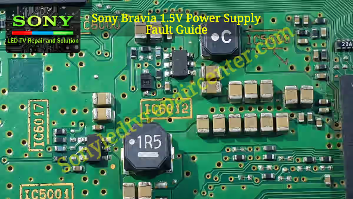
The purpose of using this model is to give a clear and realistic reference so that technicians can directly relate the explanation to an actual board instead of just theory. By studying this section step by step, it becomes easier to understand how the 1.5V rail supports the system IC and what kind of behavior the TV shows when this voltage is missing or unstable.
Role of 1.5V Supply in MediaTek IC
In Sony Bravia KLV-40W652D main board, a MediaTek system IC is used, and the 1.5V supply is a core requirement for its proper operation. This voltage helps power the internal digital core of the IC where the actual processing begins. Without this voltage, the system IC cannot enter a stable working state, which results in no boot or a dead TV condition.
This 1.5V line also supports different internal blocks of the system IC, such as CPU core logic, data processing section, and internal communication paths. This is the stage where the main control logic of the TV runs, and even a small voltage drop can push the system into hanging or restart loop issues. That is why in repair work, this rail is considered very critical and must remain stable for proper operation.
Sony Bravia KLV-40W652D 1.5V Supply Details
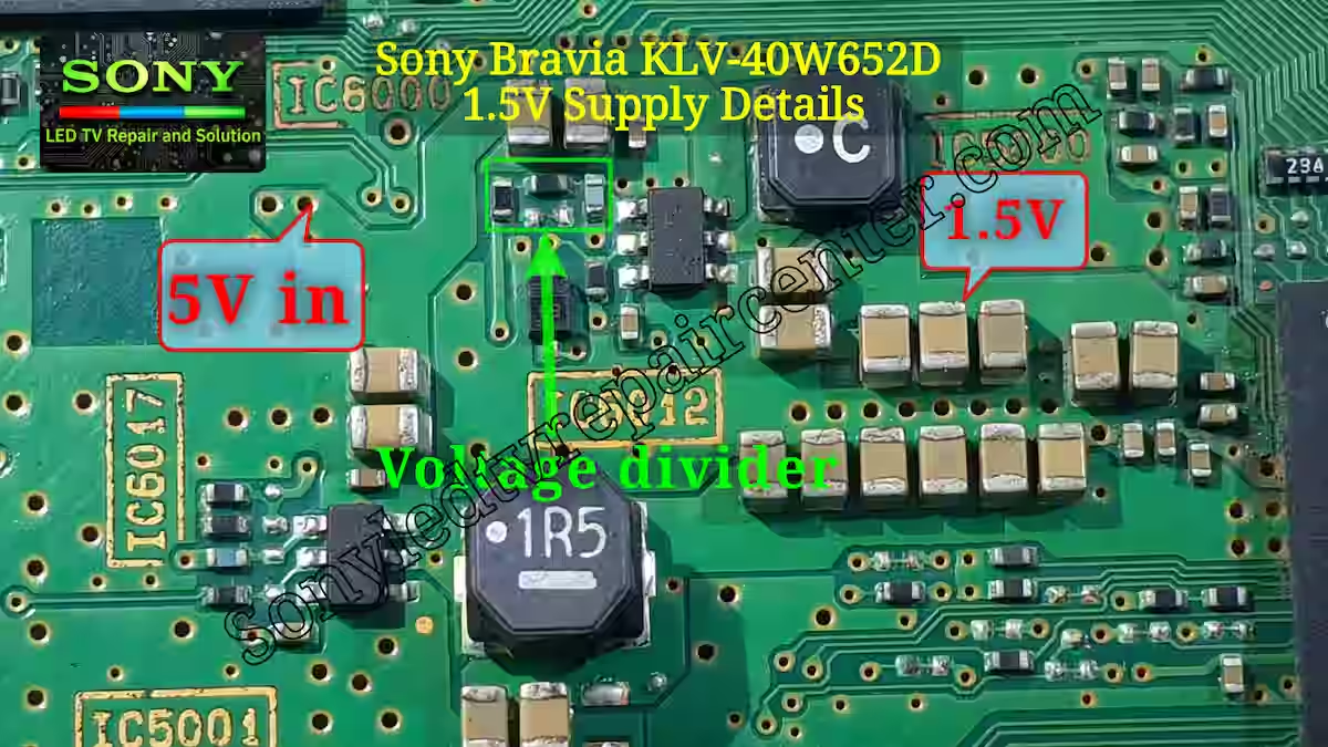
In the Sony Bravia KLV-40W652D main board, a buck converter IC 6012 is used to generate the 1.5V supply. Proper operation of this IC is very important for the entire 1.5V section. It has a total of 6 pins, and each pin has its own specific function. Pin 1 is ground, Pin 2 is LX output which generates the output voltage through the inductor, and Pin 3 receives the 5V input supply from the system IC. This stage mainly starts the conversion process where a higher voltage is stepped down into a stable 1.5V line.
Pin 4 is the feedback pin which plays a main control role in voltage regulation. A voltage divider network of resistors is connected to this pin to sense the output voltage and send a control signal back to the IC. Pin 5 is the Enable (EN) pin which controls ON/OFF operation of the IC, meaning the regulator can switch between active and standby mode through this pin. Pin 6 is connected with a ceramic capacitor that helps in stability, ripple control, and noise filtering. From a repair point of view, the most critical section is the feedback network, because even a slight change in resistor value can cause the 1.5V line to go up or down, resulting in system IC instability. That is why technicians should always check feedback resistors, output short conditions, and feedback line continuity carefully, as most faults originate from this area.
Real Repair Experience with 1.5V Section
From my practical experience working on Sony Bravia 1.5V sections, I have noticed that most of the issues in this model come from feedback resistor value drift. This feedback network usually consists of a voltage divider made with three resistors. One resistor comes from the output line, another is in series and connects to the feedback pin (Pin 4) of the IC, and the third one is connected from the feedback line to ground. This reference setup is very sensitive, and even a slight change in resistor value can disturb the regulation of the 1.5V line. In some cases, this disturbance not only affects stability but can also damage the buck converter IC and sometimes even stress the main system IC.
I have also seen cases where ceramic capacitors on the output side become short and create a heavy short condition on the 1.5V rail. There are multiple capacitors connected on this line, and any one of them can go short, so proper checking is very important. In a few repairs, I had to replace the main buck converter IC itself because it was damaged due to excessive load or feedback failure. Another point I have observed is that some boards use different current ratings in similar IC designs, especially in low-cost versions, but Sony typically uses higher-grade components for better stability. However, if a lower-rated replacement is used, it may work for some time but fails again later. That is why I always recommend using the original or proper equivalent component with correct rating to ensure long-term reliability.
Related Article
This Sony Bravia voltage series is part of a continuous repair guide collection created by Sony LED TV Repair Center Lahore. The purpose of this series is to explain different power supply sections of Sony Bravia main boards in a practical way, based on real repair experience. In upcoming parts, more voltage sections of the same model will also be covered so technicians can understand the complete power sequence step by step instead of isolated information.
For better understanding, you can also check the Sony Bravia 5V Power Supply Detail and the Sony Bravia 3.3V Power Supply Fault Guide,Sony Bravia 1.2V Power Supply Fault Guide, which are already part of this same voltage series.
1.5V Buck Converter Block Diagram
This section explains the basic working structure of the 1.5V buck converter in a simplified way for better understanding. It is only a reference block diagram, and the actual IC configuration may vary depending on the board design.
Pin 1 is ground, while pin 2 is the switching node where a 4.7µH coil is connected. This inductor plays a key role in energy storage and smoothing the output voltage, which is then supplied to the system IC. Pin 4 is used for feedback (FB), which helps the IC maintain a stable regulated output by monitoring the output voltage level.
In this example, the compensation network consists of resistors R1 (4.2K), R2 (3K), and R3 (3.2K), which are connected toward the feedback section to stabilize regulation. Pin 6 is the bootstrap (BST) pin, pin 3 is the input supply pin where 5V is applied, and pin 5 is the enable (EN) pin used to turn the regulator ON or OFF.
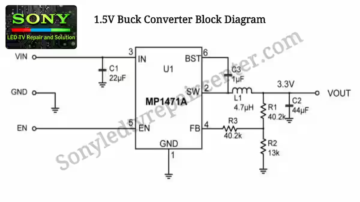
This explanation is based on a typical reference design to help understand the working principle of the buck converter stage used in Sony Bravia main boards.
Conclusion
The Sony Bravia 1.5V Power Supply Fault Guide gives a clear understanding of how this specific voltage rail plays an important role in the overall functioning of the main board. In real repair practice, proper checking of this section helps a lot in identifying hidden faults that are often missed during basic troubleshooting.
This guide, based on practical repair experience from Sony LED TV Repair Center Lahore, is part of a complete voltage series where each section is being explained step by step. Understanding these details not only makes fault finding easier but also improves repair accuracy in real working conditions.
Sony KDL-40W600B No Power Fault Guide

Shaukat Ali has over 30 years of experience in LED TV repair, specializing in chip-level repair work. He is an expert in Sony LED TVs, and also repairs other major brands like Samsung, TCL, Orient, and Haier. His expertise includes display panel faults, motherboard issues, power supply circuits, T-Con, and HDMI faults. Based in Lahore, he shares real-time fault finding cases from daily repair work to help technicians and learners with practical experience.
📞 Contact: +92 321 4066054