
ST5461B05 Panel Scaler Test Points
NT61312H-C6518A-A COF Data is a complete reference article for this COF, compatible with the ST5461B05 panel. In this guide, you will find full COF data along with COF test points and scaler strip test points, all covered in one place for easy understanding and practical use.
This article is designed to give you a clear and complete view of both COF and scaler side signals, so you can easily trace lines, check voltages, and understand the panel behavior during fault finding. Both sections are explained with proper reference to help technicians and learners work more accurately.
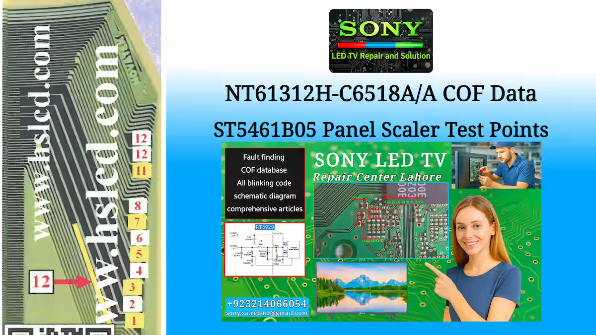
Side COF Function in Panel
Side COF (Chip-on-Film) is a critical part of the panel that handles signal transfer from the T-con or main board to the display lines on one side of the screen. It drives the gate and data signals that control how pixels turn ON and OFF, so the image forms correctly. In simple terms, this section is responsible for managing a specific portion of the panel, making sure that area displays properly without distortion.
If the side COF develops a fault, the issue usually appears only in the area it controls. You may see vertical lines, half display problems, or one side completely blank while the rest of the screen works fine. That’s why understanding the role of side COF is important, especially for beginners, because it helps in quickly identifying whether the fault is related to the panel side or coming from another section.
ST5461B05 Panel Scaler Strip Test Points
Below, we are providing the image of the scaler strip for this panel, where all the test points are clearly marked. These points help you understand the signal flow and voltage positions on the scaler side, making it easier to perform measurements and trace faults during practical work.
By following the marked test points in the image, you can quickly identify important lines and check their behavior. This is especially useful when working on panel-related issues, as it gives you a clear reference of the scaler section in one view.
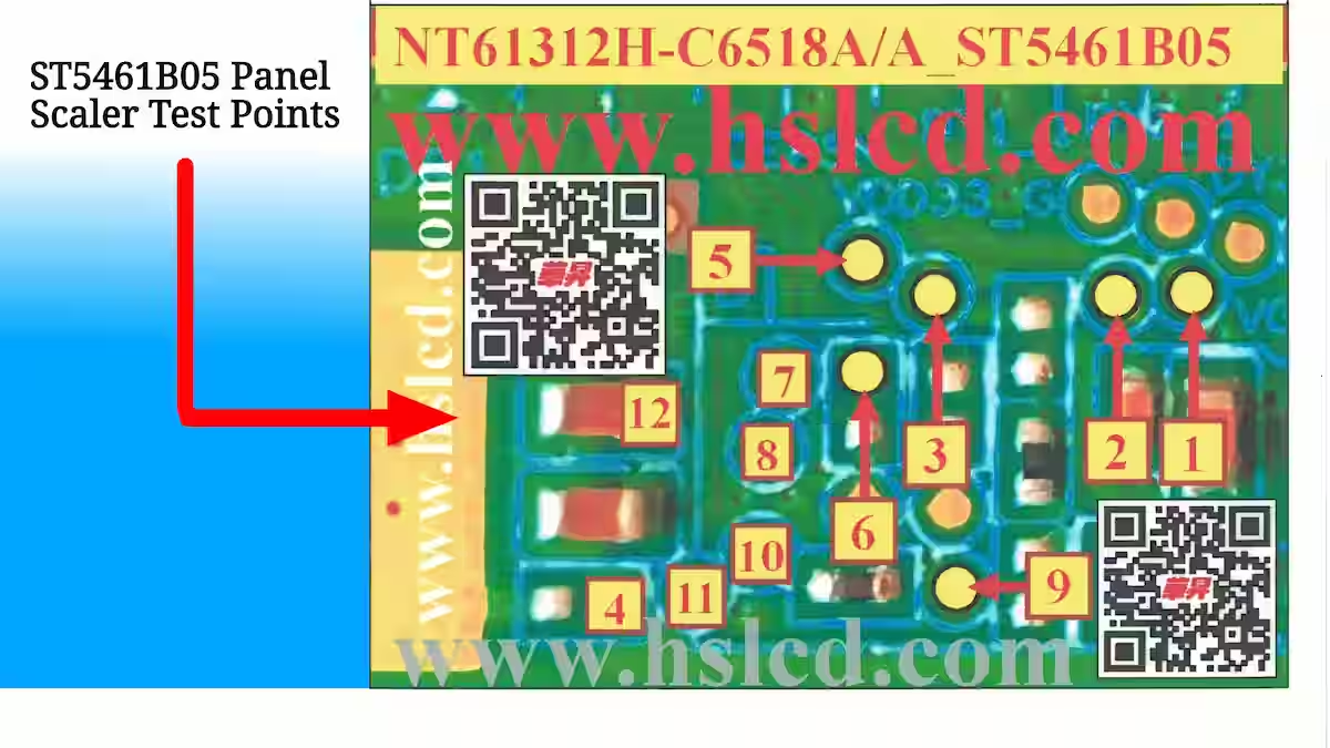
NT61312H-C6518A-A COF Data image
Below, we are presenting a complete image that includes both COF test points and scaler strip test points along with their voltage details. This combined reference gives you a full overview in one place, so you can easily see all signal lines, test points, and their corresponding voltages without needing multiple sources.
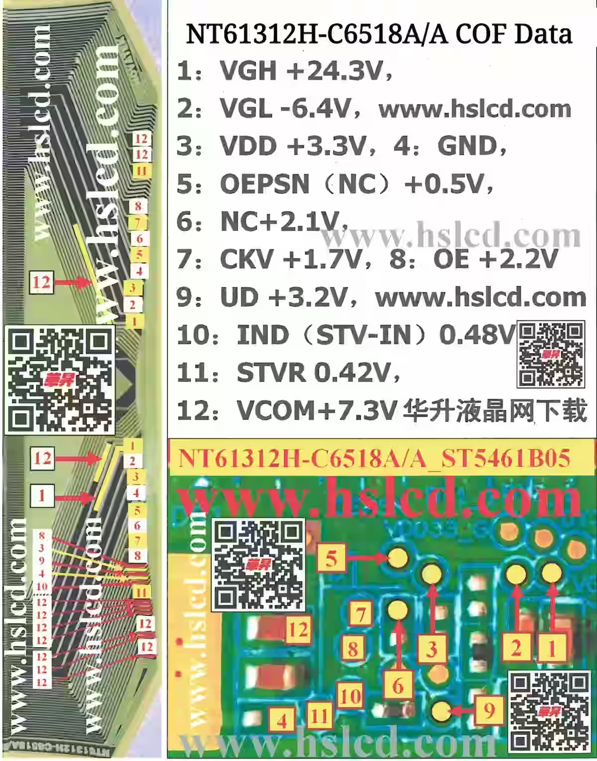
This image acts as a complete package for this panel, helping you quickly trace signals, verify voltages, and understand how both COF and scaler sections are working together during troubleshooting.
COF Test Points Description with Voltage
1 VGH – +24.3V
VGH is essential for driving the vertical gate lines in the panel. It provides the high-level voltage required to switch the TFT pixels ON properly during scanning. This ensures that each vertical line is activated at the correct timing and the image is formed clearly on the screen.
If VGH voltage is missing, low, or unstable, the panel will not be able to drive the vertical lines correctly. This can result in vertical lines missing, half display, complete blank screen, or severe flickering issues across the panel.
2 VGL – -6.4V
VGL is required to turn the vertical gate lines OFF properly in the panel. It provides the negative voltage needed to control pixel discharge and maintain correct scanning balance. This helps the panel generate a stable and accurate display without unwanted pixel activation.
If VGL voltage is missing, too low, or unstable, the gate lines may not turn OFF properly. This can cause vertical lines, dark or uneven display areas, flickering, or partial image distortion on the screen.
3 VDD – +3.3V
VDD is the main supply voltage for the COF logic circuit. It powers the internal control IC that manages signal processing and pixel driving. This voltage is essential for stable operation of the panel, ensuring that data signals are correctly received and distributed across the display.
If VDD voltage is missing, low, or unstable, the panel may stop working properly. This can cause a completely blank screen, random flickering, no display response, or partial image failure depending on how the COF section is affected.
4 GND – 0V
GND is the ground reference for the COF circuit. It completes the electrical path for all voltages in the panel and provides a stable reference level for proper signal operation. Without a proper ground, none of the supply voltages can work correctly.
If GND is loose, broken, or unstable, the panel may behave unpredictably. This can lead to flickering, distorted display, random lines, or complete loss of picture depending on how badly the ground connection is affected.
5 OEPSN (NC) – +0.5V
OEPSN in this case is marked as NC (No Connection), but still shows a small reference voltage around +0.5V. Even though it is not a main driving line, it can still be part of internal biasing or monitoring inside the COF structure.
If this voltage is unstable or completely missing, it usually does not affect the full panel directly, but in some cases it may cause minor instability in signal behavior or slight irregular display response depending on the panel design.
6 NC – +2.1V
NC (No Connection) pins are generally not used for direct signal driving, but in some panels they still carry a reference voltage like +2.1V. This voltage may be part of internal biasing or support circuitry within the COF structure.
If this voltage becomes unstable or disappears, it usually does not create a major fault in the display. However, in some cases it can cause slight signal disturbance or minor instability depending on the panel design and COF configuration.
7 CKV – +1.7V
CKV is the clock signal used in the COF to control the timing of data transfer to the panel. It ensures that pixel data is shifted and displayed in proper sequence during each scan cycle. A stable CKV is very important for correct image formation.
If CKV voltage is missing, weak, or unstable, the panel may show horizontal lines, distorted image, flickering, or complete display failure in severe cases because the timing sequence of pixels gets disturbed.
8 OE – +2.2V
OE (Output Enable) controls when the COF drivers are allowed to send data to the panel pixels. It works as a switching signal that enables proper pixel activation according to timing control from the scaler section. This signal is important for stable and synchronized display output.
If OE voltage is missing, low, or unstable, the panel may show no display, partial image, flickering, or uneven screen response. In some cases, certain sections of the display may not update properly, leading to half or broken picture behavior.
9 UD – +3.2V
UD (Up/Down) is used to control the scanning direction of the gate lines in the panel. It ensures that the pixel driving sequence follows the correct order so the image is displayed properly from top to bottom. This signal plays an important role in maintaining correct display orientation and stable scanning.
If UD voltage is missing, incorrect, or unstable, the panel may show reversed image behavior, incorrect line scanning, vertical distortion, or uneven display response. In some cases, the picture may appear unstable or partially misaligned depending on the fault condition.
10 IND (STV) – 0.48V
IND (STV) is the start pulse signal for the vertical scanning process in the COF. It initiates the gate driver sequence so that pixels are activated line by line in a proper order. This signal is very important for starting and maintaining correct vertical scanning of the panel.
If IND (STV) voltage is missing, low, or unstable, the panel may fail to start scanning properly. This can result in no display, vertical lines missing, half screen blank, or unstable image flickering depending on the fault condition.
11 STVR – 0.42V
STVR is a vertical reset / return signal used in the panel driving sequence. It helps in resetting and synchronizing the vertical scanning process so that each frame starts correctly from the top line. This signal ensures proper timing control between successive scanning cycles.
If STVR voltage is missing, incorrect, or unstable, the panel may show vertical scrolling issues, improper frame reset, flickering display, or partial/no image depending on the fault condition. It can also disturb overall vertical synchronization and result in unstable picture behavior.
12 VCOM+ – 7.3V
VCOM+ is a reference voltage used in the LCD panel to control pixel driving balance. It works with the VCOM circuit to maintain proper voltage levels across the liquid crystal so that the pixels can switch correctly between bright and dark states. This voltage is very important for stable and clear image formation.
If VCOM+ voltage is missing, incorrect, or unstable, the display may show flickering, washed-out picture, uneven brightness, or flick lines on the screen. In severe cases, the panel may show distorted or unstable images because pixel switching becomes unbalanced.
Technical Advice
While bypassing a side COF, it is strongly recommended that both side tracks should be properly disconnected. If a technician bypasses only one side and leaves the other side connected, the issue may temporarily be resolved, but after some time the same fault can reappear again. Proper isolation of both sides ensures stable repair and long-term reliability of the panel.
The purpose of providing all the pin descriptions above is to create awareness for technicians, so they can clearly understand the function and role of each point in the panel operation. When you know the actual function of a signal or voltage, it becomes much easier to diagnose and properly handle COF or panel-related faults during repair.
This article is being published for technicians and beginners to help improve their understanding of LCD/LED panel troubleshooting. We will continue sharing such technical articles for learning purposes on behalf of Sony LED TV Repair Center Lahore.
Related Articles
If you want to read more COF data reference articles and panel scaler test points, you can read more detailed technical guides from the links below for better understanding and practical troubleshooting in real field work: Read More: [NT61305H-C52A3A Datasheet].
If you want to read more COF data reference articles and panel scaler test points, you can read more detailed technical guides from the links below for better understanding and practical troubleshooting in real field work: Read More: [HV550QUB-B11 Side COF Data].
If you want to read more COF data reference articles and panel scaler test points, you can read more detailed technical guides from the links below for better understanding and practical troubleshooting in real field work: Read More: [NT61303H-C52A2B DATA SHEET].
Conclusion
This is a complete reference article of NT61312H-C6518A-A COF Data, specifically designed and fully compatible with the ST5461B05 Panel Scaler Test Points panel model. In this NT61312H-C6518A-A COF Data guide, all essential technical details have been clearly explained, including pin-wise voltage information, COF test points, and scaler strip test points for proper field troubleshooting. The main purpose of this article is to provide accurate and practical guidance to technicians during real repair work.
The goal of this COF DATA article is to help both technicians and beginners clearly understand the function and importance of each signal and voltage within the ST5461B05 Panel Scaler Test Points system. Without proper testing knowledge and signal understanding, COF or panel-level repair can become difficult and unreliable, so this complete reference serves as a strong practical learning resource for fault diagnosis and repair work.
Sony Bravia 3.3V Power Supply Fault Guide

Shaukat Ali has over 30 years of experience in LED TV repair, specializing in chip-level repair work. He is an expert in Sony LED TVs, and also repairs other major brands like Samsung, TCL, Orient, and Haier. His expertise includes display panel faults, motherboard issues, power supply circuits, T-Con, and HDMI faults. Based in Lahore, he shares real-time fault finding cases from daily repair work to help technicians and learners with practical experience.
📞 Contact: +92 321 4066054