
Working Function Explanation IC RT6929
RT6929 IC Comprehensive Details This is used in the DC to DC panel of TFT. It meets the voltage and signal requirements of the panel. In this article, we will explain its working principle. We will also explain its pin details with the help of a schematic diagram and block diagram. We will also explain its input voltage and output voltage in simple terms so that even a common technician can understand the working principle of this IC. Sony LED TV Repair Center Lahore has started a whole series in which different ICs will be published.
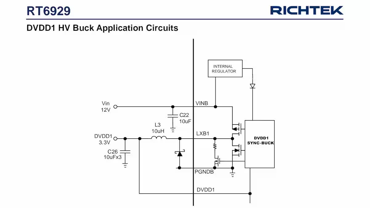
DVDD1-3.3 Buck circuit
The DVDDD1 voltage is generated inside the IC itself, and the input for it is twelve volts, as you can see in the image below. A point emerges from inside the IC, LXB1, and the voltage is stabilized by connecting an inductor coil L3 2.2 uH to the point, grounding a ten uF capacitor. This voltage is used at different places in the panel.
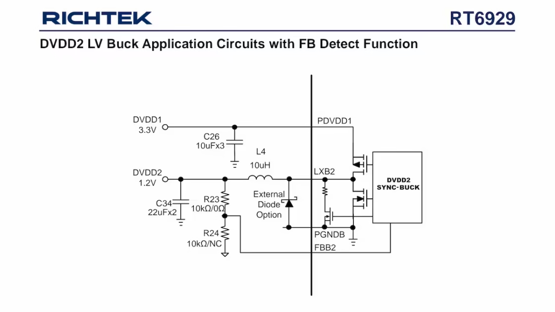
DVDD2 Circuit FB with detect
This power supply is generated inside the DVDD2 1.2 V IC. An inductor coil L4 is placed in front of pin LXB2, and a 22 µF ceramic capacitor is grounded. The special thing about this circuit is that its feedback voltage divider is external. It keeps the voltage stable. Its input voltage is 3.3V.
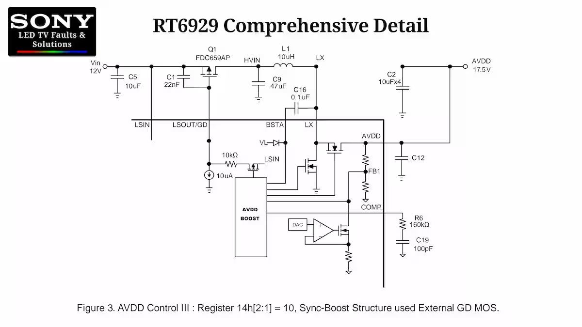
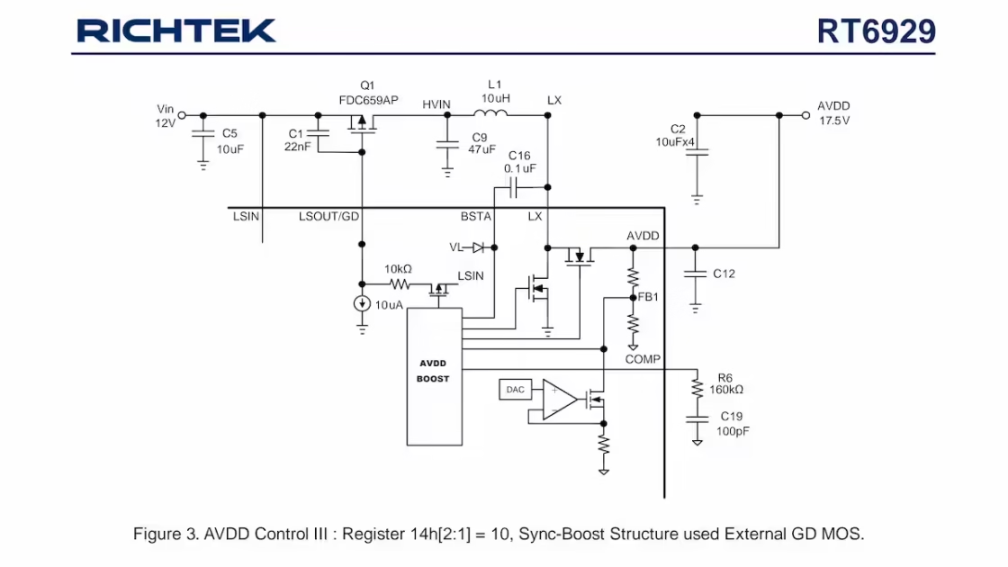
AVDD 17.5 V boost up circuit
This 12 V boosted-up AVDD supply goes to the LX pin of the IC in series with an inductor coil through a MOSFET. Here, about thirty volts are boosted, and two MOSFETs inside the IC control this voltage and provide 17.5 volts. Their feedback circuit is inside the IC itself.
Pin description
1 VINB–Supply Input Pin for Buck Converter DVDD1 (3.3V).
2 NC–No Internal Connection.
3 LXB1–Switching Node of Buck Converter DVDD1 (3.3V).
4 PGNDB–Power Ground of 3.3VDD, 1.2VDD Buck Converter.
5 LXB2–Switching Node of 1.2VDD Buck Converter.
6 PDVDD1–Power Input of 1.2VDD Buck Converter.
7 DVDD1–Power for 1.8VDD LDO & Feedback of Buck Converter DVDD1 (3.3V).
8 DVDD3–Output of 1.8VDD LDO.
9 FBB2–Feedback of 1.2VDD Buck Converter.
10 VCC–Power for RESET, Inverter.
11 RESET–RESET Signal Output from the integrated DVDD1 (3.3V) Voltage Detector.
12 CDLY–RESET Signal Delay Adjustment Point. The value of the capacitance on this Pin Sets the Time Delay for the RESET Output.
13 EN–Enable Signal Input of 3.3VDD, 1.2VDD Buck Converter, 1.8VDD LDO.
15 TRDY–Enable Signal Input from T-CON.
16 BANK_SEL–Bank Select Input for AVDD, HAVDD, DVR and AVDD trimming of 2D/3D; Bank_Sel = 0 => Output Bank 1 = 2D Bank_Sel = 1 => Output Bank 2 = 3D
17 SDA_OUT–Analog Switch Output. (Connect with T-CON I2C interface)
18 SCL_OUT–Analog Switch Output. (Connect with T-CON I2C interface)
19 SDA_IN–I 2C Compatible Serial-Data Input. Analog Switch Input. (Connect with Connector only)
20 SCL_IN–I 2C Compatible Serial-Clock Input. Analog Switch Input. (Connect with Connector only)
21 INV_OUT–Inverting Output from Integrated Inverter. (INV_IN function Pin is EN_ASW/WPN Pin)
22 EN_ASW/WPN–Enable/Disable for the Integrated Analog Switch. Active Low is AVDD Trimming and DVR Writing Protection. 0 = Prevent I2C Data Writes to Internal AVDD Trimming & DVR EEPROM but allow register writing. 1 = Allow I2C Data Writes to Internal AVDD Trimming & DRV EEPROM and Register
23 SEQ_IN–Enable/Disable for AVDD and HAVDD.
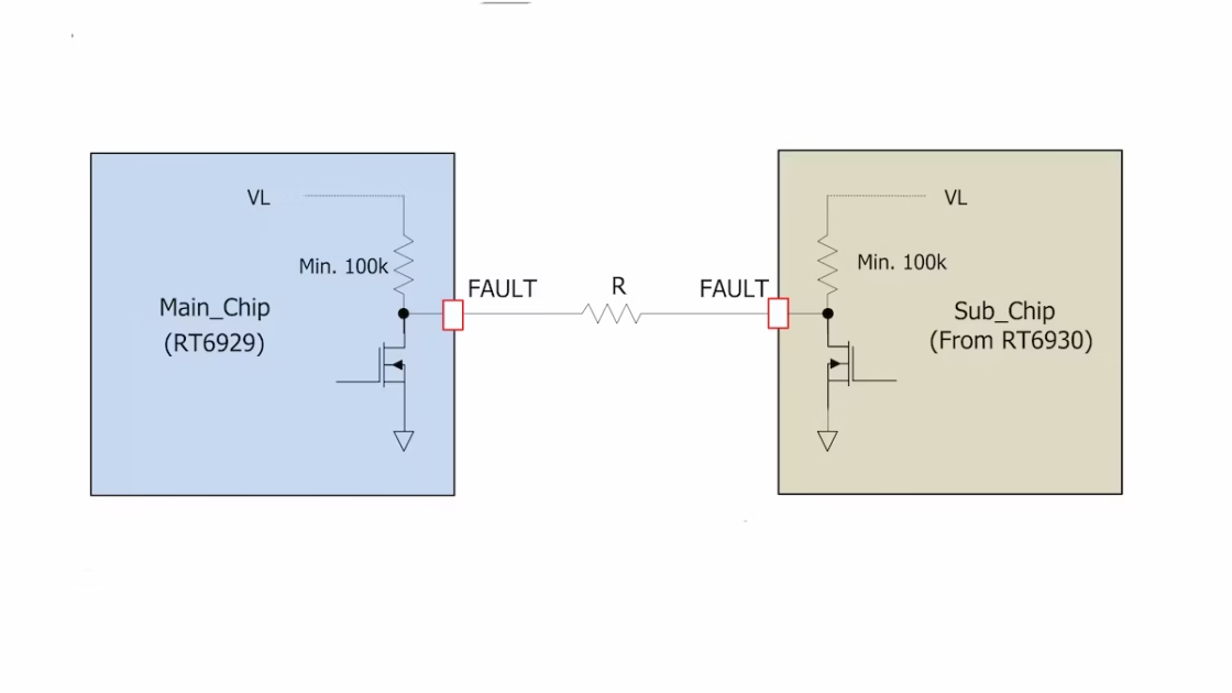
24 FAULT–FAULT Signal (DATA EN, SCP, TSD, UVLO) Output & Enable Signal Input.
25 T_SENSE–Temperature Sense Pin.
26 A0–Slave Address Assignment.
27 C_GND–Ground of Amplifier.
28 VCOM3–Output of VCOM Amplifier 3.
29 NEG3–Negative Input of VCOM Amplifier 3.
30 VCOM2–Output of VCOM Amplifier 2.
31 NEG2–Negative Input of VCOM Amplifier 2.
32 VCOM1–Output of VCOM Amplifier 1.
33 NEG1–Negative Input of VCOM Amplifier 1.
34 POS3–Positive Input of VCOM Amplifier 3.
35 DVR_REF–DVR Reference Input.
36 VINO–Power Input of VCOM Amplifier.
37 HAVDD–HAVDD Buck Feedback Input & Amplifier Output.
38 LXH–Switching Node of HAVDD Buck Converter.
39 PGNDH–Power Ground of HAVDD Buck Converter.
40 LSIN–Load Switch Input & Power Input of HAVDD Buck Converter.
41 LSOUT/GD–Load Switch Output or Gate Drive Pin for External P-MOSFET.
42 PGND–Power Ground of AVDD Boost Converter.
43 LX–Switching Node of AVDD Boost Converter.
44 BSTA–Bootstrap Capacitor Connection of AVDD Boost Converter.
45 AVDD–AVDD Boost OUTPUT & Feedback Input.
46 AGND–Analog Ground.
47 COMP–Compensation Pin for AVDD Boost Control Loop.
48 VL–Internal Linear Regulator Output. Connect this pin with a decoupling capacitor.
49 (Exposed Pad) GND–Ground. The Exposed Pad must be soldered to a large PCB and connected to GND for maximum power dissipation.
RT6929 programmable 12C interface
This IC is programmable and works through a 12C interface. It has a memory flash in which its data is stored. I mean, if this IC is used with a Sony board, it will also connect to the main board through clock data. This IC also communicates with the Next IC Bomber RT6930 on the same principle. We have written a separate article on RT6930. You can read it.
RT6929 Fault function
During normal operation, each fault pin becomes a high state. If the one chip becomes the fault state, the fault pin becomes the low state. Thus, the fault pin of the other chip also becomes low-state and shuts down. If the RT6929 becomes the fault state, the RT6930 becomes shut down. If the RT6930 becomes the fault state, the RT6929 becomes shut down except for logic power. If the resistor R is removed, the fault pin of the other chip becomes high-state and normal operation. As shown in Figure 29.
Layout Consideration RT6929
PCB layout is very important for designing power switching converter circuits. For best performance of the RT6929, the following layout guidelines must be followed: For good regulation, place the power components as close as possible. The traces should be wider and shorter, especially for the high current output loop. The feedback voltage divider resistors and output sense voltage pin must be near the feedback pin. The divider’s center trace and output sense voltage pin must be short and avoid the trace near any switching nodes.
Complete PDF Preview File Zoom and Scroll
Conclusion
RT6929 IC Comprehensive Details We have explained this DC-to-DC IC with our best effort. There may be many points left out, but considering the length of the article, we have covered only the essential points. Yes, there will be more pictures in this article because without them, this topic would have been incomplete. There are still many pictures that have been left out. Sony LED TV Repair Center Lahore will continue to bring such helpful articles for you.
How to Fix Sony XR-55X90J 4 Blink Error
BD9423EFV IC PDF Pinout & Diagram
Sony KDL-60W600B All Blink Codes Details

Shaukat Ali has over 30 years of experience in LED TV repair, specializing in chip-level repair work. He is an expert in Sony LED TVs, and also repairs other major brands like Samsung, TCL, Orient, and Haier. His expertise includes display panel faults, motherboard issues, power supply circuits, T-Con, and HDMI faults. Based in Lahore, he shares real-time fault finding cases from daily repair work to help technicians and learners with practical experience.
📞 Contact: +92 321 4066054