
Panda3851 Panel Scaler Test Points
8656-MC607 COF Data & Test Points is a complete and practical reference guide for the Panda3851 panel, specially prepared for technicians who want accurate COF data and reliable scaler test points in one place. In this guide, you will find detailed scaler strip information, complete test point layout, and essential voltage details for better understanding. All pin connections and signal paths are explained in a simple and technician-friendly way, making it easier for both beginners and experienced technicians to perform fast and accurate fault finding during repair work.
8656-MC607 COF Side COF Role
Side COF data is very important for proper panel operation because it handles voltage distribution and signal transfer across the display. It mainly controls the left-to-right pixel driving lines, ensuring that each column receives the correct data signal for proper image formation. This helps in accurate horizontal scanning and smooth picture display on the screen. It also supports key panel voltages and maintains stable communication between the control section and the display matrix. Without proper side COF function, the panel cannot operate in a stable way and display performance becomes disturbed.
Source COF Role
Source COF plays a key role in the panel by handling the main data signals that are sent to the display pixels. It controls the vertical pixel driving lines, ensuring that each row receives accurate image data for proper screen formation. This section works closely with the timing and data driver system to maintain correct image sequencing and color accuracy. It also helps in transferring video data from the main board to the panel matrix in a controlled and stable way. If Source COF is not functioning properly, the panel may show no display, vertical lines, or a fully distorted image output.
8656-MC607 COF Scaler Test Points
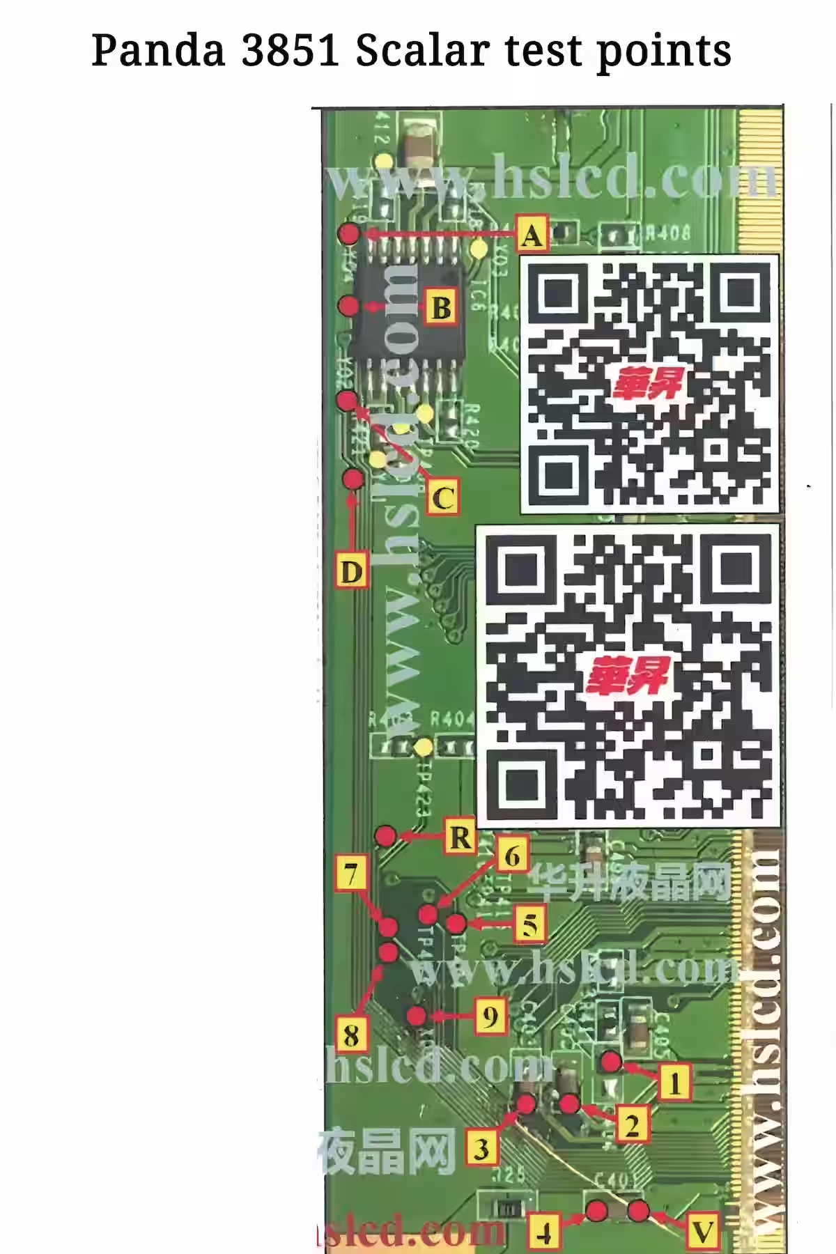
In the image below, you can see the scaler test points of the 8656-MC607 COF, where all connections of the scaler strip are clearly shown for proper understanding. This section includes complete signal lines and voltage paths used in the panel display system. By using this reference, technicians can easily identify and trace scaler-related connections for accurate fault finding and repair work on the panel.
8656-MC607 COF Overview Image
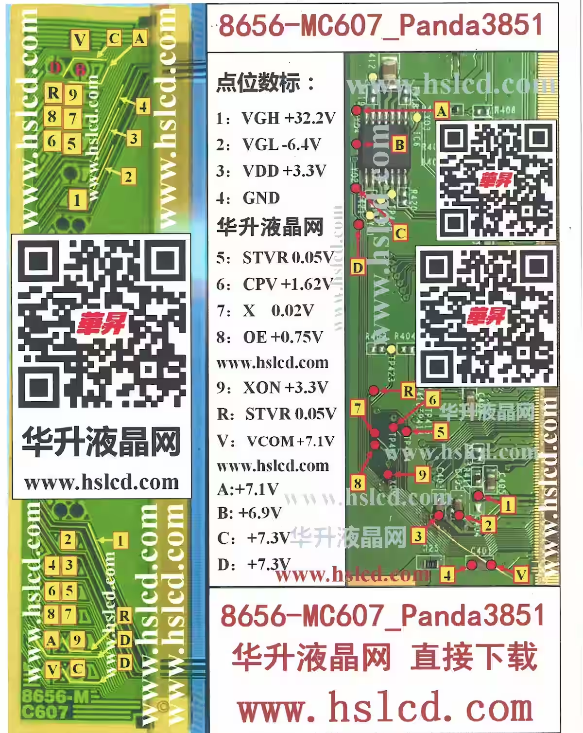
In the image below, you can see a clear overview of the 8656-MC607 COF data for Panda3851 panel, where both COF test points and scaler strip test points are shown together in a single reference image. This combined layout gives a proper understanding of the full panel connection system, including signal lines and voltage distribution points. With this image, technicians can easily trace the overall structure and perform accurate fault diagnosis in a practical repair environment.
8656-MC607 COF Pin Description
- Pin 1 VGH 32.2V
This voltage is used for the gate driving section of the TFT panel and plays a key role in turning pixel lines ON properly. It provides high-level switching voltage to the gate driver IC, which ensures correct row activation during display scanning. If this voltage is missing or low, the panel may show no display, blank screen, or completely failed image formation.
- Pin 2 VGL -6.4V
This voltage is used for the gate OFF driving control in the TFT panel and works opposite to VGH. It helps in properly switching pixels OFF by providing negative voltage to the gate driver section during scanning. If this voltage is missing or unstable, the panel may show flickering, distorted image, or improper line control on the display.
- Pin 3 VDD +3.3V
This is the main logic supply voltage for the panel control circuits and timing controller section. It powers the internal processing system that manages signal timing and data distribution across the display. If this voltage is missing or low, the panel may remain dead, not start properly, or show no display at all.
- Pin 4 GND
This is the main ground reference for the panel circuit and provides the return path for all operating voltages. It ensures stable working of VGH, VGL, VDD, and all signal lines inside the panel system. If the ground connection becomes weak or open, the panel may show unstable display, random flickering, or complete failure to operate.
- Pin 5 STVR 0.05V
This is a vertical start/reset timing signal used for frame scanning control in the TFT panel. It helps initialize each display frame and ensures proper row-by-row scanning starts in sequence. If this signal is weak, missing, or unstable, the panel may show no display, broken scanning, or vertical line distortion on the screen.
- Pin 6 CPV +1.62V
This is the clock pulse signal for the vertical scanning section of the TFT panel. It works as a timing control line that drives the gate shift operation step by step during frame display. If this signal is missing or unstable, the panel may show flickering, distorted lines, or no proper image formation on the screen.
- Pin 7 X 0.02V
This line appears to be a reference or dummy test point used for panel internal calibration or signal tracking. It does not carry a strong driving voltage like VGH or VGL, but is part of the internal checking or communication path within the COF section. If this point is abnormal or unstable, it may indicate signal loss in the driver section, which can result in missing lines, unstable display, or partial image issues on the screen.
- Pin 8 OE +0.75V
This line is the Output Enable signal for the panel driving section and plays an important role in controlling data activation. It allows pixel data to pass from the driver IC to the display matrix in a properly timed sequence. If this voltage is low, missing, or unstable, the panel may show half display, weak image, or complete loss of picture depending on the affected section.
- Pin 9 XON +3.3V
This line is used as an enable control signal for the panel driving system and helps in activating internal timing and data processing functions. It works as a switching signal that allows proper operation of the source and gate driving sections in coordination with the main control IC. If this voltage is missing or unstable, the panel may not start properly, or it may show no display or irregular screen behavior.
- Pin R STVR 0.05V
This is a vertical reset/start timing signal used for frame initialization in the TFT panel. It controls the proper reset sequence of the gate driver so each new frame can start scanning in correct order. If this signal is weak, missing, or unstable, the panel may show no display, improper vertical scanning, or random line disturbance on the screen.
- Pin VCOM +7.1V
This is the common voltage reference used for pixel balancing across the TFT panel. It plays a key role in maintaining proper charge distribution so the image stays stable, clear, and flicker-free. If this voltage is incorrect or unstable, the screen may show flickering, washed colors, uneven brightness, or complete display distortion.
- Pin A +7.1V
This line is part of the panel analog supply section and helps in supporting stable operation of the display driving circuitry. It provides a reference voltage for internal analog processing and signal conditioning within the COF system. If this voltage is missing or unstable, the panel may show abnormal display behavior such as flickering, distorted image, or no proper screen output.
- Pin B +6.9V
This line is used as an auxiliary supply voltage for the panel driving section and helps in stable operation of internal analog and driver circuits. It supports proper signal processing and maintains balance in the COF driving system. If this voltage becomes unstable or missing, the panel may show flickering, weak display, or abnormal image distortion on the screen.
- Pin C +7.3V
This line is part of the auxiliary supply section used in the panel COF system and supports stable operation of internal driver and signal processing circuits. It helps maintain proper voltage balance across the panel driving stages for smooth image formation. If this voltage is missing or unstable, the panel may show flickering, uneven display, or distorted picture output.
- Pin D +7.3V
This line is an auxiliary supply voltage used in the panel COF system and helps in maintaining stable operation of internal driving and signal processing circuits. It supports proper voltage balance across the display driving stages to ensure smooth image formation. If this voltage is missing or unstable, the panel may show flickering, uneven brightness, or distorted display output.
Personal Experience
From my experience, technicians should handle the panel with extreme care during repair work, as even slight pressure or rough handling can damage the display structure. If VGH or VGL bypass is required in side COF, the correct method is to properly isolate the faulty track by cutting it from both the scaler strip side and the COF side, and then making a controlled bypass using jumper wires. This method helps in achieving a more stable and long-lasting repair. In many cases, technicians only bypass a single broken line on the glass side, but this approach usually works for a short time and later the panel develops the same fault again or becomes completely damaged.
Conclusion – 8656-MC607 COF Data & Test Points
In conclusion, 8656-MC607 COF Data & Test Points for Panda3851 panel provides a complete and practical guide for understanding the full COF structure, scaler test points, and detailed pin voltage information. This reference helps technicians clearly analyze signal flow, voltage distribution, and panel driving behavior in real repair situations. With proper understanding of this data, fault finding becomes faster, more accurate, and more reliable, especially when working on COF and scaler-related issues in the panel.
Related Articles
If you want to read more COF and chip-on-film data articles, you can explore our other technical guides for better understanding of different panel test points and repair methods. To continue reading, you can click on the link provided below.
8658-HC528 Side COF Datasheet–Read More
NT39563H-C6502 COF DATA–Read More
Sony KLV-46BX450 6 blink error solution

Shaukat Ali has over 30 years of experience in LED TV repair, specializing in chip-level repair work. He is an expert in Sony LED TVs, and also repairs other major brands like Samsung, TCL, Orient, and Haier. His expertise includes display panel faults, motherboard issues, power supply circuits, T-Con, and HDMI faults. Based in Lahore, he shares real-time fault finding cases from daily repair work to help technicians and learners with practical experience.
📞 Contact: +92 321 4066054