
HV550QU2-B305 Side COF Pin Details and Voltage Analysis
The NT39538H-C12B9C COF DATA Pin Details are an essential part of understanding the Chip-on-Film (COF) in an LED or LCD panel, as they handle signal flow and voltage distribution. There are two types of COFs in a panel: the source COF and the side COF. In this guide, we focus on the NT39538H-C12B9C Side COF, providing a detailed look at the PCB test points for panel number HV550QU2-B305. This information is designed to help technicians troubleshoot more effectively. To illustrate the details clearly, we will include two images along with a high-definition viewport.
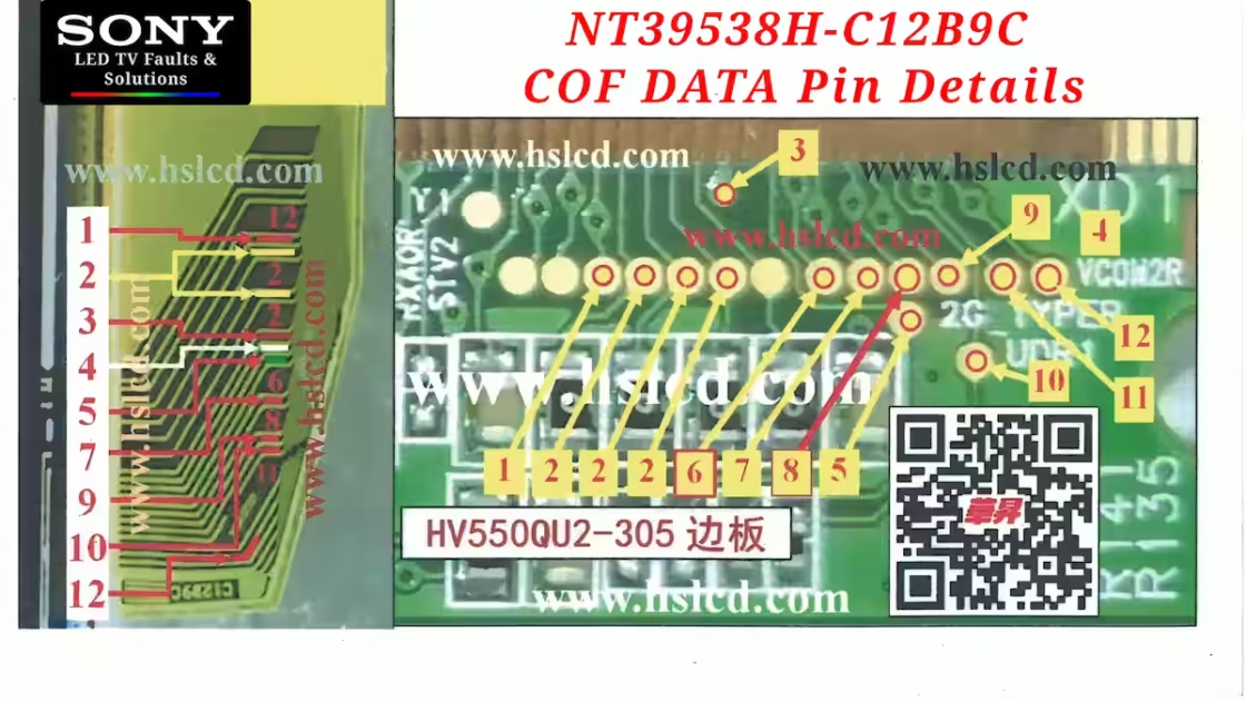
COF Pin Voltages and Picture Effect
VGH +31V
This is the Gate. High voltage is used to turn TFT pixels ON. If it drops, you may see half a screen, a dim display, or vertical lines. If it rises too high, distortion and noise appear.
VGL -7.8V
This is the Gate. Low voltage that keeps pixels OFF. If it is not low enough, ghosting or double shadows appear. If too low (more negative), flickering and fine lines can show up.
VDD +3.3V
The main logic supply powers the COF IC. Low voltage can cause freezing, a dim screen, or no display. High voltage can overheat or damage the COF.
GND (Common Ground)
Reference ground for all signals. Poor grounding causes noise, flickering, or random lines on the panel.
TYPER +0.14V
Timing reference point for internal COF operations. If unstable, it can cause shaking, jitter, or irregular line movement on the screen.
STV +0.064V
Start vertical timing pulse. If missing or unstable, the panel may show rolling, jumping, or misaligned rows.
CPV +1.4V
Clock pulse for driving rows. Incorrect level causes flickering, double lines, or partial row activation issues.
OE1 0.69V
Output enable control. If wrong, pixel response becomes unstable, and parts of the image may look faded or delayed.
XAO +3V
Panel enable/disable signal. If missing, the panel may stay black or show no activity at all.
L/R +3.27V
Left/right shift control. Wrong value can flip the image, shift rows, or cause mirrored patterns.
STV +0.06V
(Second STV line) Another vertical start reference. If unstable, it leads to row misalignment or jumping lines.
VCOM +8.2V
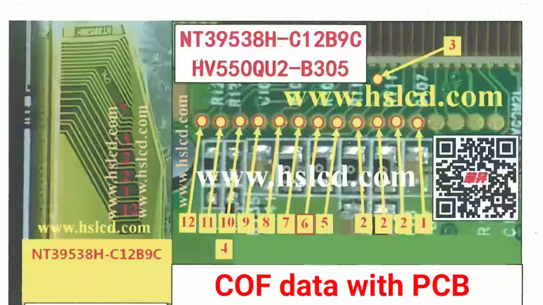
Panel PCB Connection Overview
In this article, we have provided a complete overview of the panel test points. As shown in the images, the panel used with this side COF includes all the connections of the scalar PCB. For an even clearer view, a PDF viewport is provided below, allowing you to see the panel in high definition and zoom or move it left and right as needed. If you need assistance, you can contact the Sony LED TV Repair Center in Lahore along with your fellow technicians. We will continue to publish content that supports you in every possible way, helping you work professionally—whether it’s our fault-finding articles, COF database, or circuit diagrams, everything is available for your reference.
Conclusion
The NT39538H-C12B9C COF DATA Pin Details, combined with the HV550QU2-305 PCB connections, provide a thorough reference for understanding the operation of this LCD panel. Each pin’s voltage, function, and effect on the display have been clearly explained, making it easier to diagnose issues such as flickering, ghosting, or uneven brightness. By carefully analyzing these pin details along with the PCB layout, technicians can pinpoint faults more accurately and ensure proper panel performance. Overall, this detailed information serves as a reliable guide for troubleshooting, maintenance, and ensuring the panel delivers optimal picture quality consistently.
KLV-46R452A Complete Red Light Blinking Guide
Nt39538h-C1260A COF Data with Scalar Info
How to Fix Sony XR-55X90J 4 Blink Error

Shaukat Ali has over 30 years of experience in LED TV repair, specializing in chip-level repair work. He is an expert in Sony LED TVs, and also repairs other major brands like Samsung, TCL, Orient, and Haier. His expertise includes display panel faults, motherboard issues, power supply circuits, T-Con, and HDMI faults. Based in Lahore, he shares real-time fault finding cases from daily repair work to help technicians and learners with practical experience.
📞 Contact: +92 321 4066054