
RT6905 IC Pinout & Complete Guide
The RT6905 IC Circuit Diagram is very useful for technicians working on the DC-to-DC power section of LED TV panels. This IC generates the required voltages for the panel and also supports the scan driver circuitry. It typically includes control sections for Gate Driver 1 to Gate Driver 3, which help drive the panel signals properly. In this article, we will present the RT6905 IC circuit diagram along with the surrounding components, their connections, and the necessary voltage details, making it easier to understand the IC and troubleshoot related panel issues.
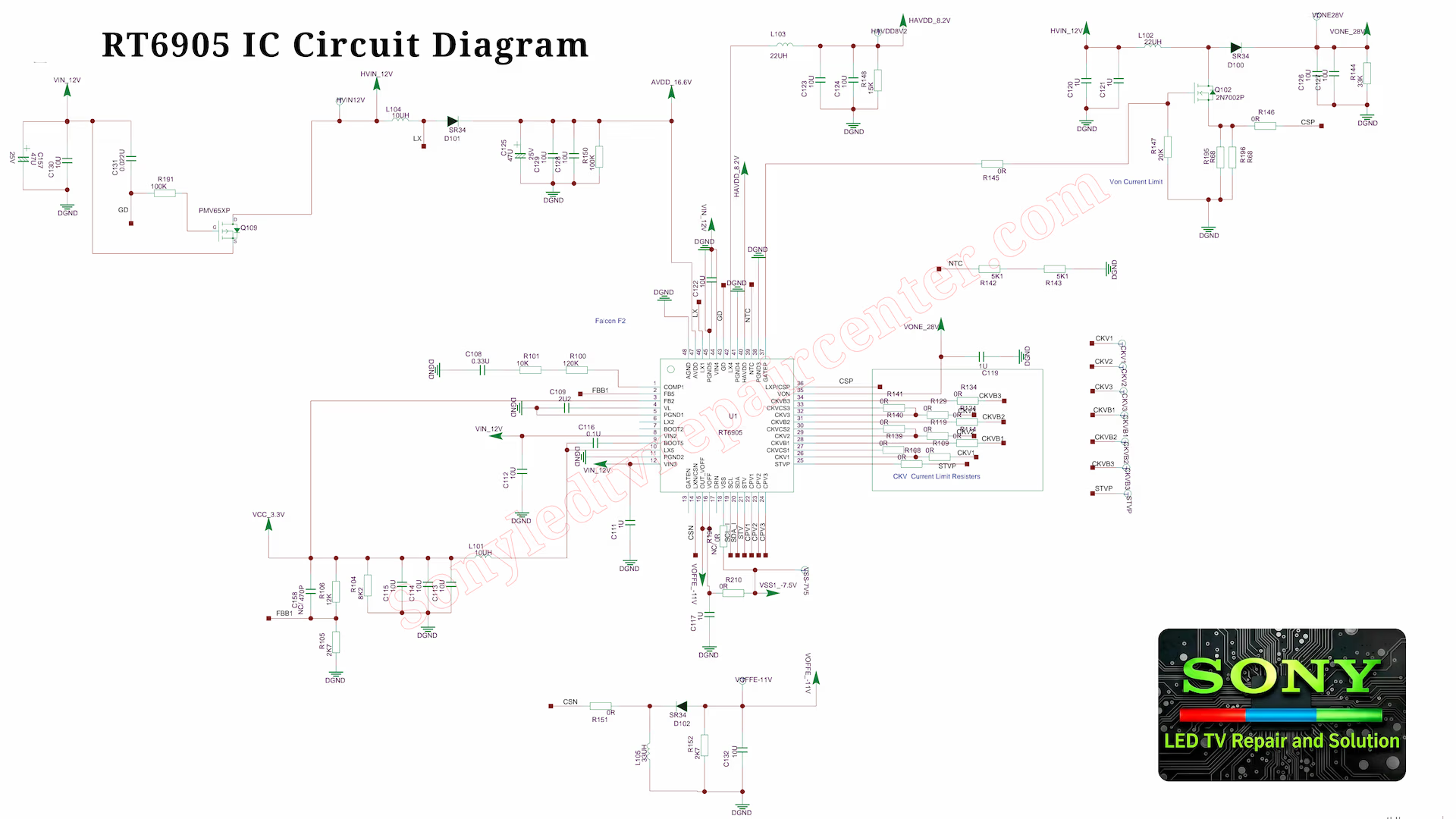
RT6905 IC Circuit Diagram PDF View
RT6905 IC Circuit Diagram Explanation
The RT6905 IC circuit diagram shows how this DC-to-DC converter works with the panel power section and the scan driver circuitry. Around the IC, several supporting components such as resistors, capacitors, and control lines are connected to regulate and stabilize the required voltages. These components help generate the proper operating voltages for the panel and ensure stable operation of the gate driver stages. By studying this circuit diagram, technicians can easily trace the voltage paths and understand how the RT6905 IC controls the panel power and driver signals.
RT6905 IC Output Voltages
VIN – 12V
VIN is the main input voltage supplied to the RT6905 IC. This voltage usually comes from the main power line and provides the primary power source for the IC to operate. The RT6905 uses this input voltage to generate different required output voltages for the panel driver and scan driver sections. A stable 12V supply at this pin is necessary for proper operation of the IC and the connected panel circuitry.
AVDD – 16.6V
AVDD is an important output voltage generated by the RT6905 IC for the panel driver circuitry. This voltage is used to power the source driver section of the LCD panel, which controls the display signals sent to the pixels. A stable AVDD voltage around 16.6V is necessary for proper panel operation and accurate image processing. If this voltage is missing or unstable, the display may show abnormal picture problems or may not operate correctly.
HAVDD – 8.2V
HAVDD is another output voltage generated by the RT6905 IC and is used to support the panel driver circuitry. This voltage helps provide the required operating power for certain driver stages inside the panel. A stable HAVDD voltage of around 8.2V ensures proper operation of the panel control circuits. If this voltage becomes low or unstable, it can affect the normal functioning of the display and may lead to picture-related issues.
VONE – 28V
VONE is an output voltage from the RT6905 IC that supplies power to specific gate driver sections of the LCD panel. With a nominal voltage of 28V, it ensures proper switching and operation of the gate transistors, which control the row lines of the display. Maintaining a stable VONE voltage is critical for accurate panel operation, and any fluctuation can result in display flickering or malfunctioning of the gate driver circuits.
VOFFE – -11V
VOFFE is a negative output voltage generated by the RT6905 IC, typically around -11V, and is used to power certain gate driver circuits in the LCD panel. This negative voltage helps the gate drivers switch correctly and ensures proper operation of the row lines. A stable VOFFE is essential for the panel’s normal functioning; any instability can lead to flickering, display errors, or improper gate driver operation.
VSS1 – -7.5V
VSS1 is a negative output voltage from the RT6905 IC, typically around -7.5V, used to provide the necessary bias for specific sections of the panel driver circuitry. This voltage ensures proper operation of the gate and source drivers, helping maintain stable signal levels across the panel. If VSS1 becomes unstable or drops, it can cause display abnormalities, flickering, or malfunctioning of the panel’s driving circuits.
VCC – 3.3V
VCC is a low-voltage output from the RT6905 IC, typically 3.3V, used to power the IC’s internal logic and control circuits. This voltage ensures that the internal digital functions, such as timing control and signal processing, operate correctly. A stable VCC is essential for proper IC performance, and any fluctuation can lead to malfunctioning of the control logic or improper operation of the panel driver circuits.
RT6905 IC Scan Driver Signals
STVP – Scan Timing Voltage Pulse
STVP is a critical signal from the RT6905 IC used to control the timing of the scan driver circuitry in the LCD panel. It synchronizes the gate drivers, ensuring that each row line is activated in the correct sequence for accurate image display. A stable STVP signal is essential for proper panel operation, as any distortion or irregularity can cause flickering, incorrect row activation, or display artifacts.
CKV1 – Clock Voltage 1
CKV1 is a clock signal output from the RT6905 IC used to synchronize the first stage of the panel’s scan driver circuitry. It provides precise timing for the gate drivers to switch row lines accurately, ensuring the correct scanning of the display. A stable CKV1 signal is crucial for proper image rendering, and any instability can result in flickering or misalignment of the displayed rows.
CKV2 – Clock Voltage 2
CKV2 is the second stage clock signal output from the RT6905 IC, responsible for controlling the timing of the next set of gate drivers in the LCD panel. This signal ensures accurate row line switching for proper scanning of the display. Maintaining a stable CKV2 is essential for smooth image rendering, and any instability can lead to flickering, timing errors, or misaligned display rows.
CKV3 – Clock Voltage 3
CKV3 is the third stage clock signal from the RT6905 IC, used to control the timing of the third set of gate drivers in the LCD panel. It ensures that the corresponding row lines are activated in the correct sequence for proper display scanning. A stable CKV3 signal is crucial for consistent image quality, and any irregularity can result in flickering, uneven rows, or display artifacts.
CKVB1 – Clock Voltage Back 1
CKVB1 is a complementary clock signal from the RT6905 IC, used in the first stage of the scan driver circuitry. It works alongside CKV1 to ensure proper timing and switching of the gate drivers for the LCD panel. A stable CKVB1 signal is essential for synchronized row scanning, and any irregularity can cause display flickering, misaligned rows, or other panel performance issues.
CKVB2 – Clock Voltage Back 2
CKVB2 is the complementary clock signal for the second stage of the scan driver from the RT6905 IC. It works together with CKV2 to ensure proper timing and synchronization of the gate drivers. A stable CKVB2 signal is essential for accurate row scanning, and any fluctuations can cause display flickering, misaligned rows, or other panel performance issues.
CKVB3 – Clock Voltage Back 3
CKVB3 is the complementary clock signal for the third stage of the scan driver from the RT6905 IC. It operates alongside CKV3 to maintain precise timing and synchronization of the gate drivers for the LCD panel. A stable CKVB3 signal is critical for smooth row scanning, and any instability can result in flickering, misaligned rows, or other display anomalies.
SCL – Serial Clock Line
SCL is the clock signal line used in the I²C communication interface of the RT6905 IC. It synchronizes the data transfer between the IC and the controlling microcontroller or processor. A stable SCL signal is essential for accurate communication, ensuring that commands and configuration data are correctly transmitted to the IC. Any irregularity in this line can lead to miscommunication, improper panel settings, or malfunction of the scan driver circuitry.
SDA – Serial Data Line
SDA is the data line for I²C communication on the RT6905 IC. It carries the actual data signals between the IC and the controller, allowing configuration of output voltages, gate driver timing, and other operational parameters. Proper functioning of the SDA line is critical for reliable IC operation, and any disturbances can cause incorrect panel behavior, improper voltage settings, or display issues.
STV – Start Pulse Signal
STV is the start pulse signal from the RT6905 IC used to trigger the scan driver sequence in the LCD panel. This signal initiates the activation of the gate driver rows in a precise order, ensuring that the panel scans correctly from the first row to the last. A stable STV signal is crucial for proper timing and synchronization of the display; any irregularity can lead to flickering, misaligned rows, or incomplete image rendering.
CPV1 – Clock Pulse Voltage 1
CPV1 is a clock pulse signal from the RT6905 IC used to control the timing of the first stage of the scan driver circuitry. It ensures that the gate drivers switch the row lines at precise intervals, allowing accurate scanning of the LCD panel. A stable CPV1 signal is essential for smooth display operation, and any instability can cause flickering, timing errors, or misaligned rows.
CPV2 – Clock Pulse Voltage 2
CPV2 is the second stage clock pulse signal from the RT6905 IC that controls the timing of the gate drivers in the LCD panel. It works in sequence with CPV1 to ensure proper row scanning and synchronization of the display. A stable CPV2 signal is critical for accurate panel operation, and any irregularity can result in flickering, uneven row activation, or display artifacts.
CPV3 – Clock Pulse Voltage 3
CPV3 is the third stage clock pulse signal from the RT6905 IC, responsible for controlling the timing of the final set of gate drivers in the LCD panel. It ensures that the corresponding row lines are activated in proper sequence for accurate scanning. A stable CPV3 signal is essential for consistent image quality, and any fluctuations can lead to flickering, misaligned rows, or other display anomalies.
Conclusion
In conclusion, the RT6905 IC circuit diagram serves as a vital roadmap for technicians and engineers working on LED TV panels. From powering the panel through its DC-to-DC conversion to driving the gate and scan circuits with precision, this IC plays a crucial role in ensuring accurate and stable display performance. Understanding its output voltages, scan driver signals, and key pins allows for efficient troubleshooting, proper voltage monitoring, and reliable operation of the panel. By following this detailed guide, anyone can gain complete insight into the RT6905 IC, making maintenance, repair, and optimization of LED TV displays far easier and more effective.
Want to master more LED TV repairs? Check out our full guides on IC troubleshooting, panel voltages, and circuit diagnostics to fix your TV like a pro!
For those interested in exploring more LED TV ICs, check out our detailed guide on the OB2273 Circuit Diagram and Detail Guide. This comprehensive article walks you through the OB2273 IC pinout, output voltages, and circuit connections, providing step-by-step explanations for troubleshooting and repair. Just like the RT6905 guide, it’s designed to help technicians and enthusiasts fully understand the IC’s functions and maintain precise control over LED TV panels.
For readers looking to expand their LED TV repair knowledge, don’t miss our BD28623MUV Audio IC Technical Guide. This guide provides a complete breakdown of the BD28623MUV IC, including pinout details, voltage outputs, and audio signal connections. With step-by-step explanations, it’s perfect for technicians and enthusiasts who want to troubleshoot and maintain high-quality audio performance in LED TV panels.
Sony KLV-40W652D 3 Blink Error Fix Guide
Sony XR vs Other TV Processors

Shaukat Ali has over 30 years of experience in LED TV repair, specializing in chip-level repair work. He is an expert in Sony LED TVs, and also repairs other major brands like Samsung, TCL, Orient, and Haier. His expertise includes display panel faults, motherboard issues, power supply circuits, T-Con, and HDMI faults. Based in Lahore, he shares real-time fault finding cases from daily repair work to help technicians and learners with practical experience.
📞 Contact: +92 321 4066054