
Sony KLV-40W652D – BD28623MUV Audio IC
BD28623MUV Audio IC Technical Guide provides complete and practical information about this Class D Speaker Amplifier for Digital Input. In this article, we will explain the working principle of the BD28623MUV Audio IC, its common faults, failure symptoms, and the important surrounding components that should be checked during repair. You will also find a clear explanation of its typical application in LED TV circuits, along with a full step-by-step description to make troubleshooting easier and more accurate. If you are working on sound-related issues, especially in models like Sony KLV-40W652D, this guide will help you understand the IC in depth and diagnose audio problems with confidence.
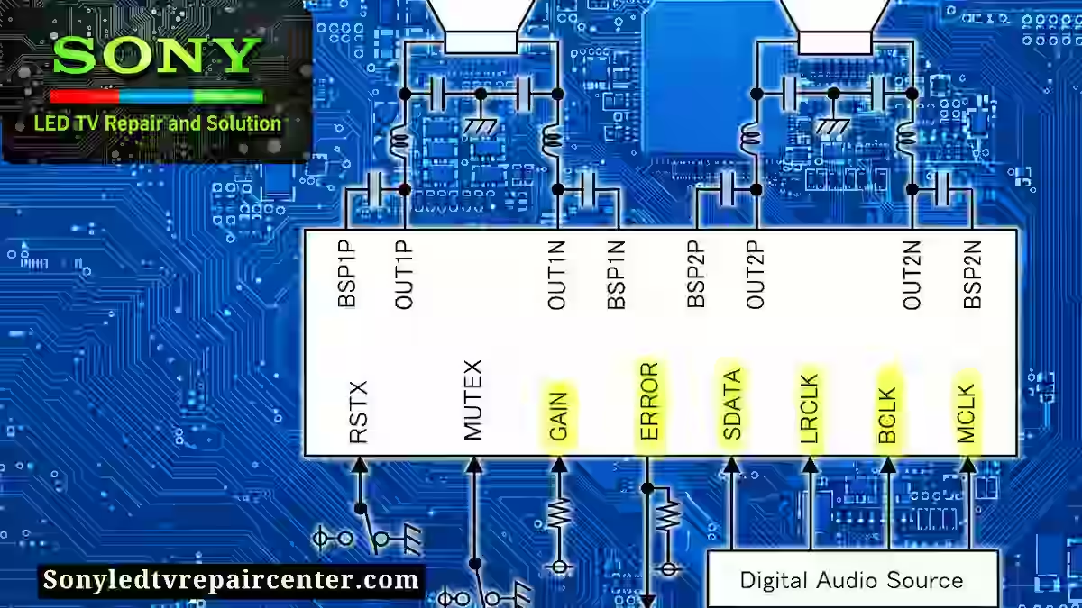
Typical Application Circuit
In the image above, you can see the typical application circuit of the BD28623MUV Audio IC Technical Guide, presented in a clear block diagram form. This diagram helps you understand how the digital audio source is connected to the IC, where the speaker outputs are taken, how the main power supply is applied, and where the mute control circuit is positioned. By studying this typical layout, technicians can easily trace the signal flow from input to output and identify the key sections involved in audio amplification. This overview makes it much easier to understand how the IC operates in an LED TV circuit before moving into detailed troubleshooting steps.
Key Features of BD28623MUV Audio IC
The BD28623MUV Audio IC is a Class D speaker amplifier designed for digital input, offering clear and high-quality sound in LED TVs. It supports I²S digital audio (16/20/24-bit) with standard LRCLK frequencies (32 kHz, 44.1 kHz, 48 kHz) and fixed BCLK, while MCLK operates at 256fS/512fS with automatic detection. The IC ensures low power consumption in RESET mode and includes a slew rate controller, removing the need for extra snubber circuits. Its output feedback circuitry keeps sound quality stable, reduces noise and distortion, and allows fewer large capacitors in the circuit. Other key features include variable gain, wide supply voltage range (8.5V–24V), soft muting, pop noise prevention, and built-in protection against overheating, under-voltage, output short, and clock stop issues. All this comes in a compact VQFN024V4040 package, making it reliable and efficient for modern LED TV designs.
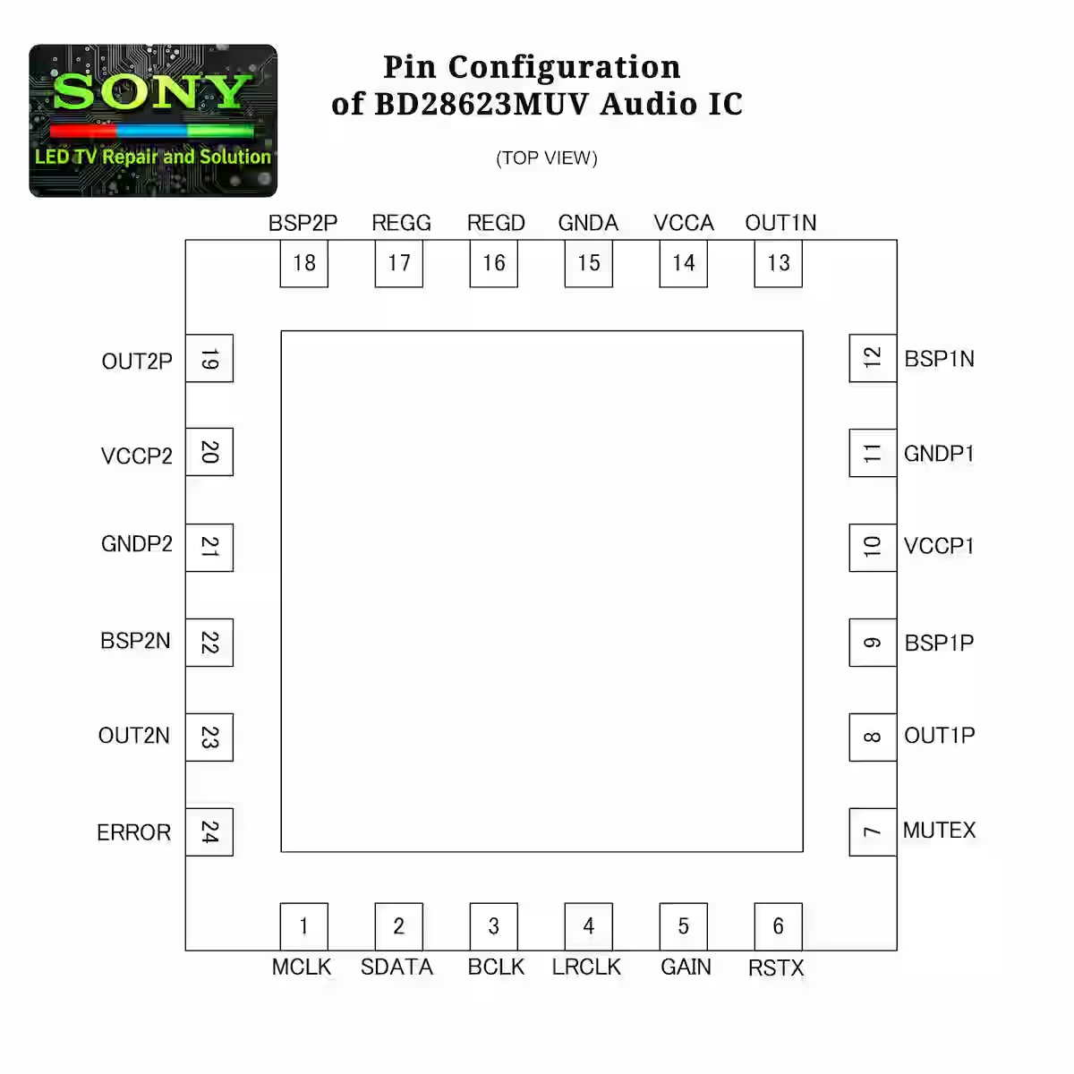
Pin Configuration of BD28623MUV Audio IC
Pin 1 – MCLK
The MCLK pin serves as the master clock input for the BD28623MUV Audio IC, providing the primary timing reference for all internal digital audio processing. It ensures proper synchronization of audio data from the digital source and stable output to the amplifier stages. If the MCLK signal is missing, unstable, or improperly connected, it can result in no sound, distorted audio, or incorrect synchronization with LRCLK and BCLK. Faulty driving circuits or voltage spikes can also damage the IC and lead to permanent audio failure.
Pin 2 – SDATA
The SDATA pin on the BD28623MUV Audio IC carries the serial digital audio data from the source to the IC, working together with MCLK, BCLK, and LRCLK to deliver accurate audio information to the amplifier. This pin ensures proper digital-to-analog conversion and maintains audio resolution and fidelity. If the SDATA signal is missing, inverted, or unstable, the IC may produce no sound, intermittent audio, or distorted output, and poor connections, broken traces, or issues in the digital audio source can all lead to SDATA-related faults, affecting overall sound quality.
Pin 3 – BCLK
The BCLK pin on the BD28623MUV Audio IC provides the bit clock signal that synchronizes the transfer of each bit of digital audio data from the source to the IC. It works in conjunction with MCLK, LRCLK, and SDATA to ensure accurate timing for digital-to-analog conversion and stable audio output. If the BCLK signal is missing, unstable, or incorrectly connected, the IC may produce distorted audio, intermittent sound, or no output at all, and faults in the clock-driving circuit or poor PCB connections can directly affect overall sound performance.
Pin 4 – LRCLK
The LRCLK pin on the BD28623MUV Audio IC carries the left-right clock signal, indicating whether the current audio data on SDATA corresponds to the left or right channel. It works together with MCLK, BCLK, and SDATA to ensure correct channel separation and accurate digital-to-analog conversion. If the LRCLK signal is missing, unstable, or incorrectly connected, the IC may produce channel inversion, distorted stereo output, or no sound from one channel, and issues in the digital audio source or broken PCB traces can lead to LRCLK-related faults.
Pin 5 – GAIN
The GAIN pin on the BD28623MUV Audio IC is used to select the amplifier’s gain level, allowing adjustment between different amplification settings such as 17dB, 20dB, or 26dB. This pin ensures the output volume matches the design requirements of the LED TV’s audio system while maintaining low distortion and consistent sound quality. If the GAIN pin is incorrectly configured, left floating, or has a poor connection, the IC may produce too low or too high output, uneven volume, or distorted sound, affecting overall audio performance.
Pin 6 – RSTX
The RSTX pin on the BD28623MUV Audio IC is the reset input, used to initialize the IC and place it into a known state during power-up or when recovering from faults. This pin helps ensure stable operation by resetting internal circuits and preventing unpredictable behavior. If the RSTX signal is missing, held low, or has intermittent contact, the IC may fail to start, produce no sound, or behave erratically, and faulty reset circuits or PCB issues can directly cause RSTX-related faults.
Pin 7 – MUTEX
The MUTEX pin on the BD28623MUV Audio IC is used for the mute control function, allowing the audio output to be temporarily silenced without powering down the IC. This pin helps prevent unwanted noise or pops during power on/off or signal transitions, ensuring smooth audio operation. If the MUTEX signal is not properly applied, left floating, or has poor connection, the IC may produce pop noise, intermittent audio, or fail to mute/unmute correctly, which can affect overall sound quality and user experience.
Pin 8 – OUT1P
The OUT1P pin on the BD28623MUV Audio IC is the positive output for the first speaker channel in the Class D amplifier configuration. It delivers the amplified audio signal to the speaker, working together with OUT1N to provide a differential output that improves sound quality and reduces noise. If OUT1P has a poor connection, short, or is damaged, the IC may produce distorted sound, low volume, or no output on the first channel, and issues in the PCB traces or connected speaker can directly affect the audio performance of this output.
Pin 9 – BSP1P
The BSP1P pin on the BD28623MUV Audio IC is the bootstrap pin for the first positive output stage of the Class D amplifier. It provides the necessary voltage swing for the high-side MOSFET driver, ensuring efficient amplification and proper operation of the OUT1P output. If BSP1P is improperly connected, floating, or has a faulty bootstrap capacitor, the IC may produce distorted audio, reduced output power, or intermittent sound on the first channel, and incorrect bootstrap circuitry can directly affect amplifier performance.
Pin 10 – VCCP1
The VCCP1 pin on the BD28623MUV Audio IC provides the main power supply for the first output stage of the Class D amplifier. It ensures that the high-power section of the IC receives stable voltage for proper audio amplification and reliable operation. If VCCP1 is missing, unstable, or has poor connections, the IC may produce no sound, distorted output, or overheating, and faults in the power supply line or PCB traces can directly impact the performance of the first channel.
Pin 11 – GNDP1
The GNDP1 pin on the BD28623MUV Audio IC serves as the ground reference for the first output stage of the Class D amplifier. It provides a stable return path for current from the OUT1P and OUT1N outputs, ensuring proper operation and minimizing noise or distortion. If GNDP1 has a poor connection, broken trace, or high resistance, the IC may produce distorted audio, intermittent sound, or unstable output voltage, directly affecting the performance and reliability of the first speaker channel.
Pin 12 – BSP1N
The BSP1N pin on the BD28623MUV Audio IC is the bootstrap pin for the negative side of the first output stage in the Class D amplifier. It provides the necessary voltage swing for the low-side MOSFET driver, ensuring proper operation and efficient amplification of the OUT1N signal. If BSP1N is improperly connected, left floating, or has a faulty bootstrap capacitor, the IC may produce distorted audio, reduced output power, or intermittent sound on the first channel, and errors in the bootstrap circuitry can directly impact the amplifier’s performance.
Pin 13 – OUT1N
The OUT1N pin on the BD28623MUV Audio IC is the negative output for the first speaker channel in the Class D amplifier configuration. It works together with OUT1P to provide a differential output, improving sound quality and reducing noise. If OUT1N has a poor connection, short circuit, or is damaged, the IC may produce distorted audio, low volume, or no output on the first channel, and faults in the PCB traces or connected speaker can directly affect the audio performance of this output.
Pin 14 – VCCA
The VCCA pin on the BD28623MUV Audio IC provides the analog power supply for the internal control and pre-amplifier circuits. It ensures stable voltage for proper operation of the audio processing stages and maintains low noise and distortion in the output signal. If VCCA is missing, unstable, or has poor connections, the IC may produce distorted sound, intermittent audio, or malfunction in control circuits, directly affecting the overall audio quality and reliability of the amplifier.
Pin 15 – GNDA
The GNDA pin on the BD28623MUV Audio IC serves as the ground reference for the analog and control circuits. It provides a stable return path for currents in the pre-amplifier and control sections, helping to maintain clean audio signals and low noise. If GNDA has a poor connection, broken trace, or high resistance, the IC may produce distorted audio, unstable operation, or erratic behavior in the control circuits, affecting overall sound quality and amplifier reliability.
Pin 16 – REGD
The REGD pin on the BD28623MUV Audio IC provides the regulated voltage output used internally for digital and control circuits. It ensures stable operation of internal logic and reduces voltage fluctuations that could affect audio processing. If REGD is missing, unstable, or improperly connected, the IC may exhibit distorted audio, erratic behavior, or malfunction of internal digital circuits, which can impact the overall performance and reliability of the amplifier.
Pin 17 – REGG
The REGG pin on the BD28623MUV Audio IC provides the regulated voltage output for the analog sections and amplifier control circuits. It ensures stable operation of the internal analog circuitry, maintaining low noise and high audio fidelity. If REGG is missing, unstable, or has poor connections, the IC may produce distorted sound, intermittent audio, or unstable analog operation, directly affecting the overall audio performance and reliability of the amplifier.
Pin 18 – BSP2P
The BSP2P pin on the BD28623MUV Audio IC is the bootstrap pin for the positive side of the second output stage in the Class D amplifier. It provides the necessary voltage swing for the high-side MOSFET driver of the second channel, ensuring efficient amplification and proper operation of the OUT2P output. If BSP2P is improperly connected, floating, or has a faulty bootstrap capacitor, the IC may produce distorted audio, reduced output power, or intermittent sound on the second channel, and issues in the bootstrap circuitry can directly impact the performance of this output stage.
Pin 19 – OUT2P
The OUT2P pin on the BD28623MUV Audio IC is the positive output for the second speaker channel in the Class D amplifier configuration. It works together with OUT2N to provide a differential output, improving sound quality and reducing noise. If OUT2P has a poor connection, short circuit, or is damaged, the IC may produce distorted audio, low volume, or no output on the second channel, and faults in the PCB traces or connected speaker can directly affect the performance of this output.
Pin 20 – VCCP2
The VCCP2 pin on the BD28623MUV Audio IC provides the main power supply for the second output stage of the Class D amplifier. It ensures that the high-power section of the second channel receives stable voltage for proper audio amplification and reliable operation. If VCCP2 is missing, unstable, or has poor connections, the IC may produce no sound, distorted output, or overheating, and faults in the power supply line or PCB traces can directly impact the performance of the second channel.
Pin 21 – GNDP2
The GNDP2 pin on the BD28623MUV Audio IC serves as the ground reference for the second output stage of the Class D amplifier. It provides a stable return path for current from the OUT2P and OUT2N outputs, ensuring proper operation and minimizing noise or distortion. If GNDP2 has a poor connection, broken trace, or high resistance, the IC may produce distorted audio, intermittent sound, or unstable output voltage, directly affecting the performance and reliability of the second speaker channel.
Pin 22 – BSP2N
The BSP2N pin on the BD28623MUV Audio IC is the bootstrap pin for the negative side of the second output stage in the Class D amplifier. It provides the necessary voltage swing for the low-side MOSFET driver of the second channel, ensuring proper operation and efficient amplification of the OUT2N signal. If BSP2N is improperly connected, left floating, or has a faulty bootstrap capacitor, the IC may produce distorted audio, reduced output power, or intermittent sound on the second channel, and errors in the bootstrap circuitry can directly affect the amplifier’s performance.
Pin 23 – OUT2N
The OUT2N pin on the BD28623MUV Audio IC is the negative output for the second speaker channel in the Class D amplifier configuration. It works together with OUT2P to provide a differential output, improving sound quality and reducing noise. If OUT2N has a poor connection, short circuit, or is damaged, the IC may produce distorted audio, low volume, or no output on the second channel, and faults in the PCB traces or connected speaker can directly affect the performance of this output.
Pin 24 – ERROR
The ERROR pin on the BD28623MUV Audio IC is used to indicate fault conditions within the IC, such as overheat, overcurrent, output short, or under-voltage. It provides a signal to the system to alert the user or control circuitry that the IC is experiencing an abnormal condition, allowing protective measures to be taken. If the ERROR pin is active, it typically means the IC has detected a fault that could affect audio performance or safety. Ignoring this signal can lead to persistent distorted sound, intermittent audio, or even permanent damage to the amplifier and connected speakers.
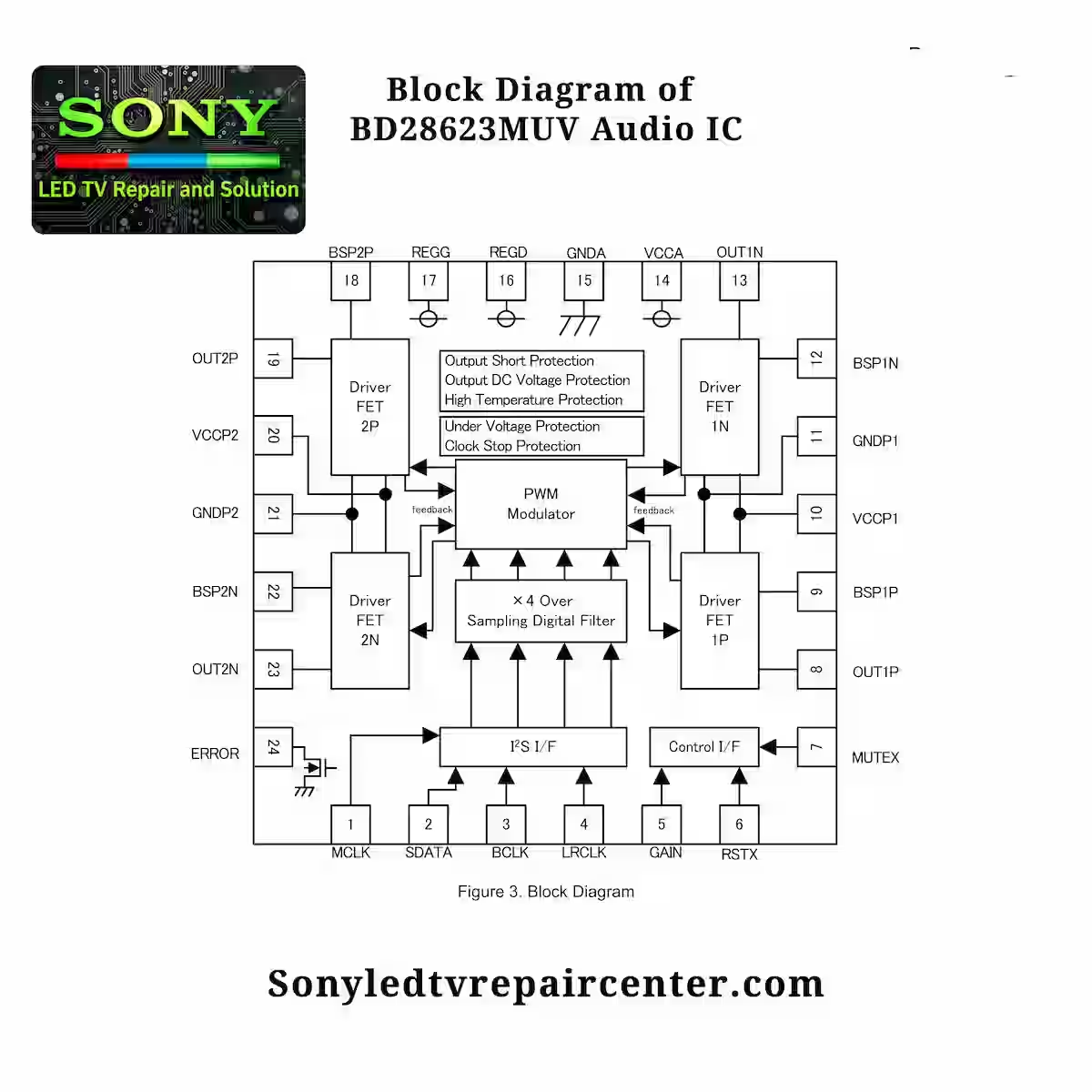
Block Diagram of BD28623MUV Audio IC
Below is Image, showing the block diagram of the BD28623MUV Audio IC. This diagram illustrates the internal structure and functional blocks of the IC, including the digital input path, speaker outputs, main power supply connections, and mute/control circuitry. It provides a clear overview of how the IC processes audio signals and manages its amplification stages, making it easier for technicians and users to understand its operation.
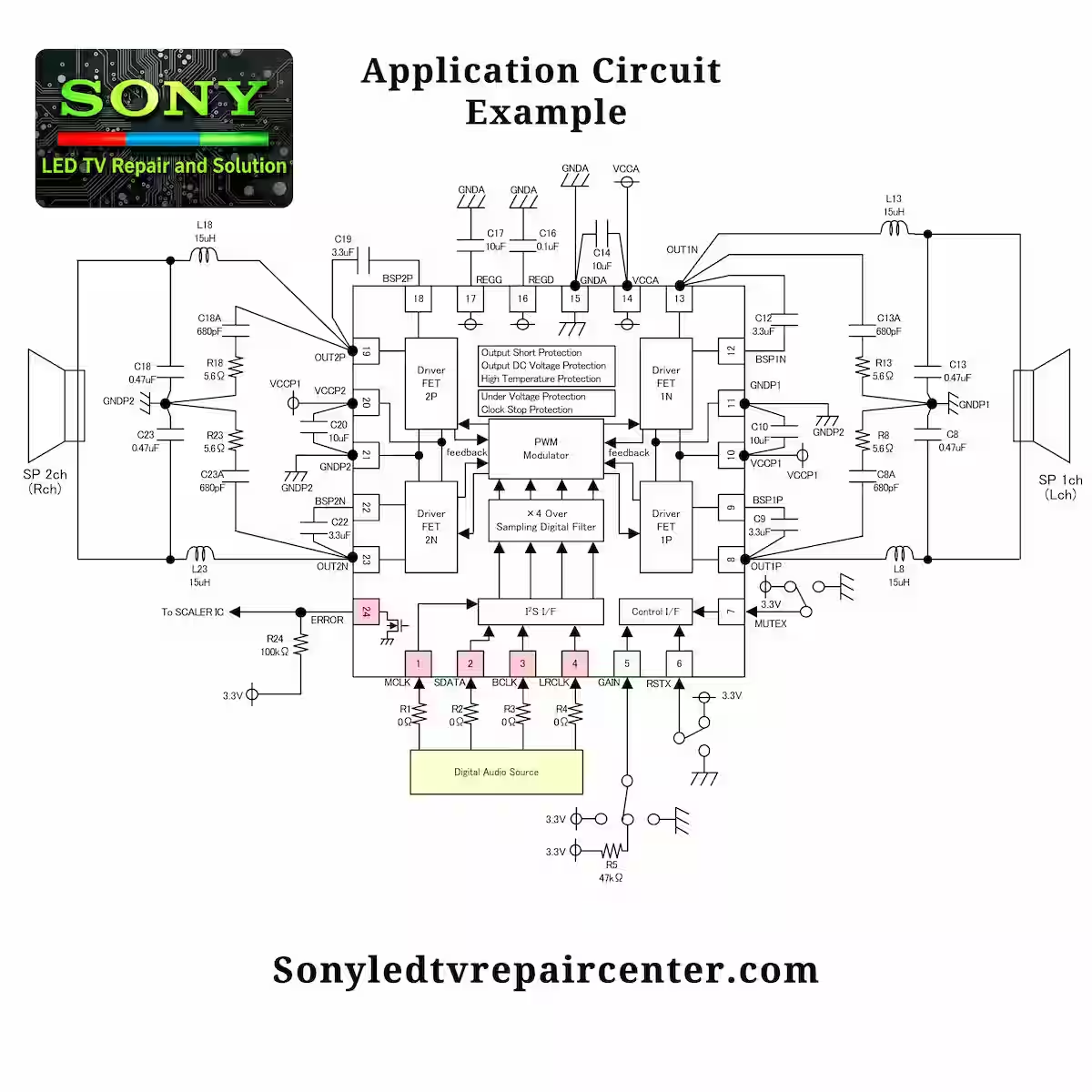
Application Circuit Example
The diagram illustrates an application circuit example for the BD28623MUV Audio IC, showing a complete setup for integrating the IC into an audio system. It highlights how the digital source communicates with the IC, the placement of the amplifier outputs to the speakers, the main power supply connections, and the mute/control circuits. This example provides a practical reference for technicians to understand typical wiring and ensure proper operation of the audio system.
Common Audio Fault in Sony KLV-40W652D
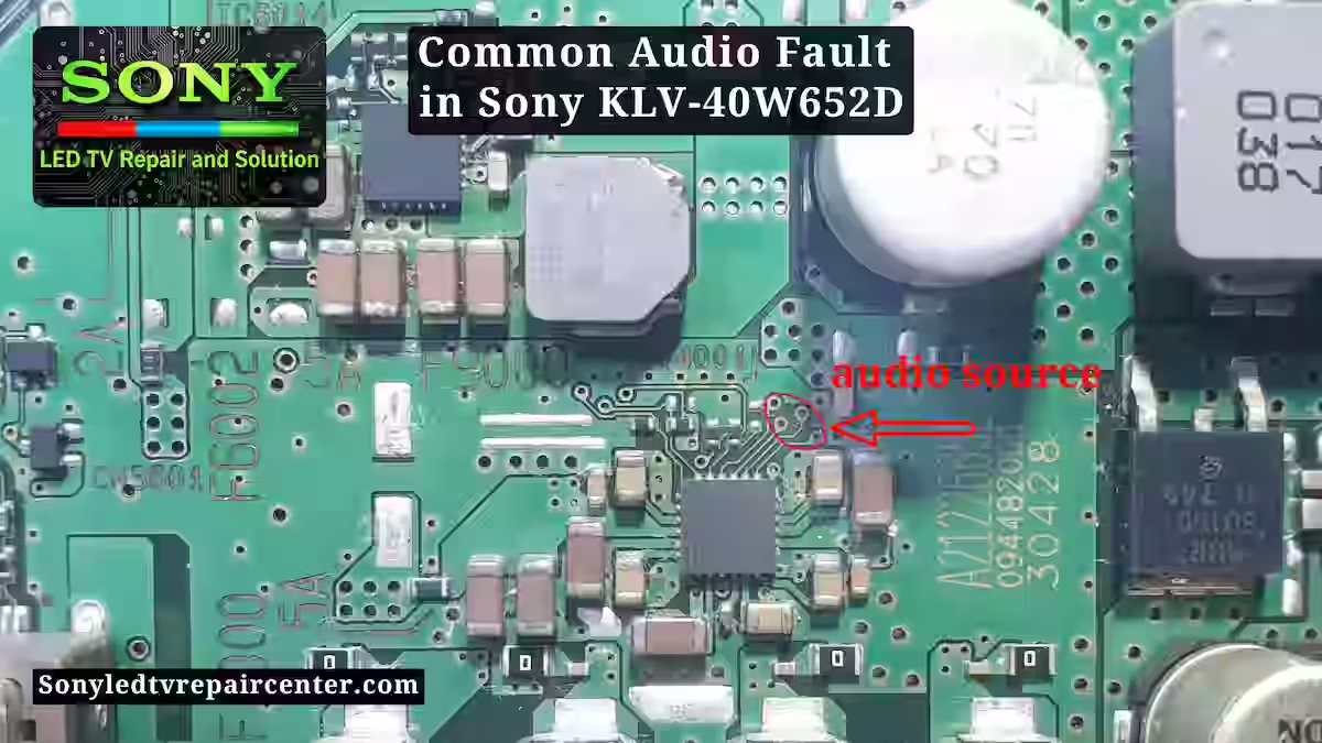
In the Sony KLV-40W652D, a common audio fault is often related to the digital audio communication between the system IC and the BD28623MUV audio amplifier IC. The digital audio source signals — MCLK (Pin 1), SDATA (Pin 2), BCLK (Pin 3), and LRCLK (Pin 4) — carry digital audio data from the system IC to the amplifier. Between these lines and the system IC, 100-ohm chip resistors are installed, usually in a single resistor array (R-Array), where all four resistors are grouped together. These resistors help maintain signal stability and proper impedance matching.
Symptoms and Troubleshooting
In many repair cases, this R-Array becomes devalued or partially faulty, which disrupts proper communication. As a result, the TV may produce noise, distorted sound, unusually high volume, or sometimes complete loss of audio. Therefore, during troubleshooting, these four signal lines and their 100-ohm resistor array must be carefully checked to ensure proper digital audio transmission. The annotated image below shows the exact pin locations on the IC for clear identification.
Conclusion
In conclusion, the BD28623MUV Audio IC Technical Guide highlights the efficiency and reliability of this Class D amplifier for digital audio applications in LED TVs. This IC, as used in the Sony KLV-40W652D model, offers low distortion, wide voltage range, and built-in protective features that ensure long-term stability. For technicians and users looking for expert guidance on Sony LED TV repair, the Sony LED TV Repair Center provides detailed insights, technical support, and practical tips to troubleshoot and maintain audio performance effectively.
SONY KD-49X7D All Blink Error Codes Guide
Sony XR vs Other TV Processors

Shaukat Ali has over 30 years of experience in LED TV repair, specializing in chip-level repair work. He is an expert in Sony LED TVs, and also repairs other major brands like Samsung, TCL, Orient, and Haier. His expertise includes display panel faults, motherboard issues, power supply circuits, T-Con, and HDMI faults. Based in Lahore, he shares real-time fault finding cases from daily repair work to help technicians and learners with practical experience.
📞 Contact: +92 321 4066054