
TPS54332 Pinout and Function Description
In this article TPS54332 Circuit Diagram & Pinout, you will find the complete TPS54332 IC schematic diagram along with detailed technical description and working explanation of this IC. This IC is commonly used in Sony LED TV power supply sections, where it plays an important role in generating stable regulated voltage for panel VCC 12V and main board circuits.
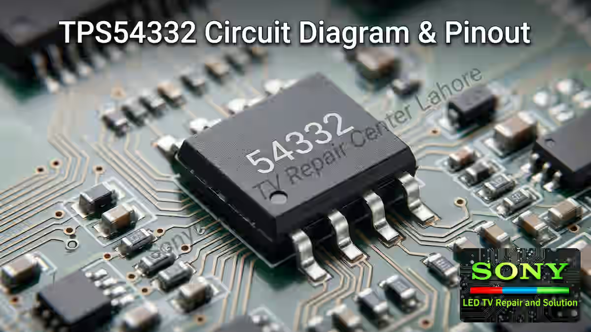
The TPS54332 is a step-down (buck) converter IC designed to convert a 19V input supply into a stable 12V output rail, which is widely used for panel VCC and main circuit sections. It ensures efficient voltage regulation with low power loss and stable performance even under varying load conditions, making it a reliable choice in modern LCD/LED TV power designs.
TPS54332 Schematic Diagram
Below schematic diagram shows the complete working structure of the TPS54332 IC circuit along with its external components. In this diagram, you can clearly observe how different parts are connected to form a complete step-down power supply system, along with component values marked for better understanding. It should be noted that the diagram shared below is an example reference, and the exact component values may vary depending on the board design, especially for the 12V output section.
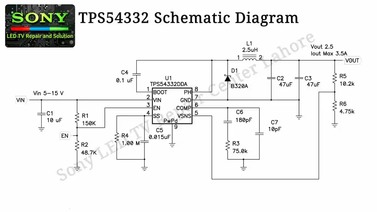
This schematic helps technicians understand how the IC processes the input voltage and generates a stable 12V output for panel VCC and main board operation, making it easier to trace the circuit and perform troubleshooting during repair work.
Simplified Schematic Diagram
This simplified schematic diagram of TPS54332 Circuit Diagram & Pinout provides an easy and clear view of the IC working structure. It is a simplified version designed to help technicians quickly understand the basic circuit flow without going into complex component-level details.
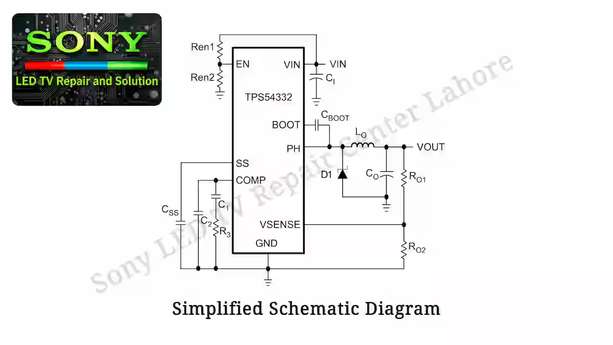
In this diagram, you can easily observe how the IC handles the input supply and generates a stable 12V output for panel VCC and main board operation. This simplified view makes it easier to understand the core functionality of the TPS54332 IC and is very useful for quick learning and basic troubleshooting.
TPS54332 PCB Layout
The below PCB layout shows the complete board-level design of the circuit, where all components are placed in their actual physical positions. In this layout, you can clearly observe the IC placement along with surrounding resistors, capacitors, and power components, which form the complete step-down converter section.
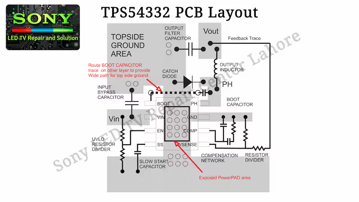
This PCB view helps technicians understand the real hardware structure and trace each connection directly on the board during repair work. It gives a practical understanding of how the IC is implemented in real circuit design. Below image shows the PCB layout for better reference and component identification.
TPS54332 Used in Sony KLV-40W652D
This IC is used in the Sony LED TV model KLV-40W652D, where it plays an important role in the power supply section by generating a stable 12V output for panel VCC and main board operation. In this model, the TPS54332 helps maintain proper voltage regulation and ensures smooth performance of the display and control circuits.
We are also writing a complete voltage detail series for this model, and as an example, we have selected the Sony KLV-40W652D to explain the full power and IC working structure in a step-by-step format. The related guide and next parts of this series can be accessed through the link provided below.
TPS54332 Pin Description
- Pin 1 – BOOTThis pin is the bootstrap supply pin for the high-side gate driver. It works together with the switching node and provides the required floating voltage to drive the high-side MOSFET. A bootstrap capacitor is connected to ensure proper switching operation and stable performance.
- Pin 2 – VINThis is the main input supply pin of the IC. It receives the 19V input voltage from the power source and feeds it into the internal regulation stage. A stable and properly filtered input on this pin is necessary for correct operation of the converter.
- Pin 3 – ENThis is the enable control pin of the IC. It is used to turn the IC ON or OFF depending on the logic level applied. When this pin is high, the IC starts normal switching operation, and when low, the IC remains in shutdown mode to save power.
- Pin 4 – SSThis pin is the soft-start control pin of the IC. It controls the ramp-up time of the output voltage during startup to avoid sudden inrush current. A capacitor is usually connected to this pin to ensure smooth and stable power-on operation.
- Pin 5 – VSENSEThis pin is the output voltage sensing input of the IC. It monitors the regulated output voltage through a feedback network and helps maintain accurate regulation. The IC adjusts its switching duty cycle based on this signal to keep the output stable.
- Pin 6 – COMPThis pin is the compensation node of the control loop. External RC components are connected here to stabilize the feedback system and improve transient response. Proper compensation ensures smooth regulation and prevents oscillations in the output voltage.
- Pin 7 – GNDThis is the ground reference pin of the IC. It provides the return path for all internal circuits and serves as the common reference point for stable operation. A solid and low-noise ground connection is essential for proper performance of the converter.
- Pin 8 – PHThis is the switching node (phase node) of the IC. It is connected to the inductor and handles high-frequency switching between input and output stages. This pin plays a key role in energy transfer and voltage conversion from 19V to 12V output.
Feedback Pin Explanation
The feedback system in the TPS54332 IC works through a simple voltage divider network connected at the output stage. In this circuit, the 12V output line is divided using two resistors (R1 and R2), where one resistor is connected from the output to the feedback line and the second resistor is connected from the feedback point to ground. The middle junction of these resistors provides a reference voltage to the IC feedback pin (VSENSE).
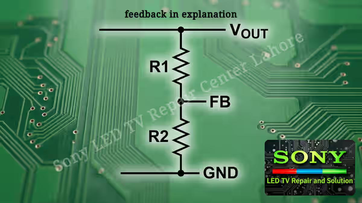
This reference voltage tells the IC how much output is being generated, and based on this feedback signal, the IC adjusts its switching operation to maintain a stable 12V output. If there is any change in the value of R1 or R2, even a small variation can directly affect the feedback voltage level, which results in a change in the output regulation. In this way, the voltage divider network plays a critical role in defining and controlling the final output voltage of the IC.
Conclusion
In this article TPS54332 Circuit Diagram & Pinout, we have covered the complete working concept of this step-down converter IC in detail. From circuit diagram and schematic explanation to pin description and feedback voltage divider network, each section is explained in a practical way to help technicians understand the real working behavior of the IC in Sony LED TV power supply boards.
Overall, the TPS54332 is a highly efficient and reliable buck converter that maintains stable 12V output for panel VCC and main board circuits. A proper understanding of its circuit structure, pin functions, and feedback operation is very useful for fault finding and accurate repair work in modern LCD/LED TV systems.
Related Article
If you want to read more detailed IC circuit diagrams and technical repair guides, you can check our other articles below. These guides will help you understand different power ICs, circuit behavior, and troubleshooting methods in a better way for practical repair work.
RT6908 IC Circuit Diagram & Technical Guide–Read More
MP3398A IC Circuit Diagram–Read More
Sony Bravia 12V Panel VCC Fault Guide

Shaukat Ali has over 30 years of experience in LED TV repair, specializing in chip-level repair work. He is an expert in Sony LED TVs, and also repairs other major brands like Samsung, TCL, Orient, and Haier. His expertise includes display panel faults, motherboard issues, power supply circuits, T-Con, and HDMI faults. Based in Lahore, he shares real-time fault finding cases from daily repair work to help technicians and learners with practical experience.
📞 Contact: +92 321 4066054