
KLV-40W652D LVDS Section Voltage Detail
In the Sony KLV-40W652D model, the LVDS section is a very important part of the display system, where the 1V regulated supply plays a key role for proper signal processing. In this Sony Bravia LVDS 1V Voltage Guide, we are focusing on the step-down regulator section that generates and controls the low voltage required by the LVDS IC.
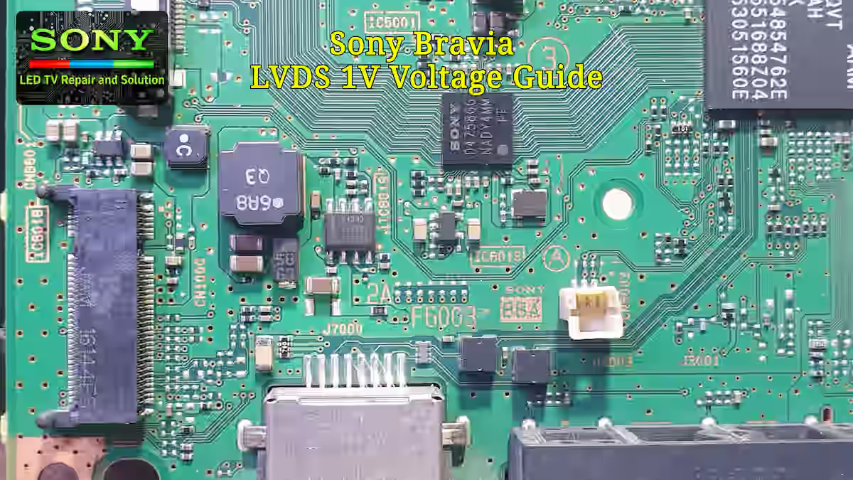
This voltage rail is not just a simple supply line; it directly supports the LVDS IC operation, which receives display data signals from the system and passes them to the panel for proper screen output. If this 1V line becomes unstable or missing, the display section can fail completely or show abnormal picture issues.
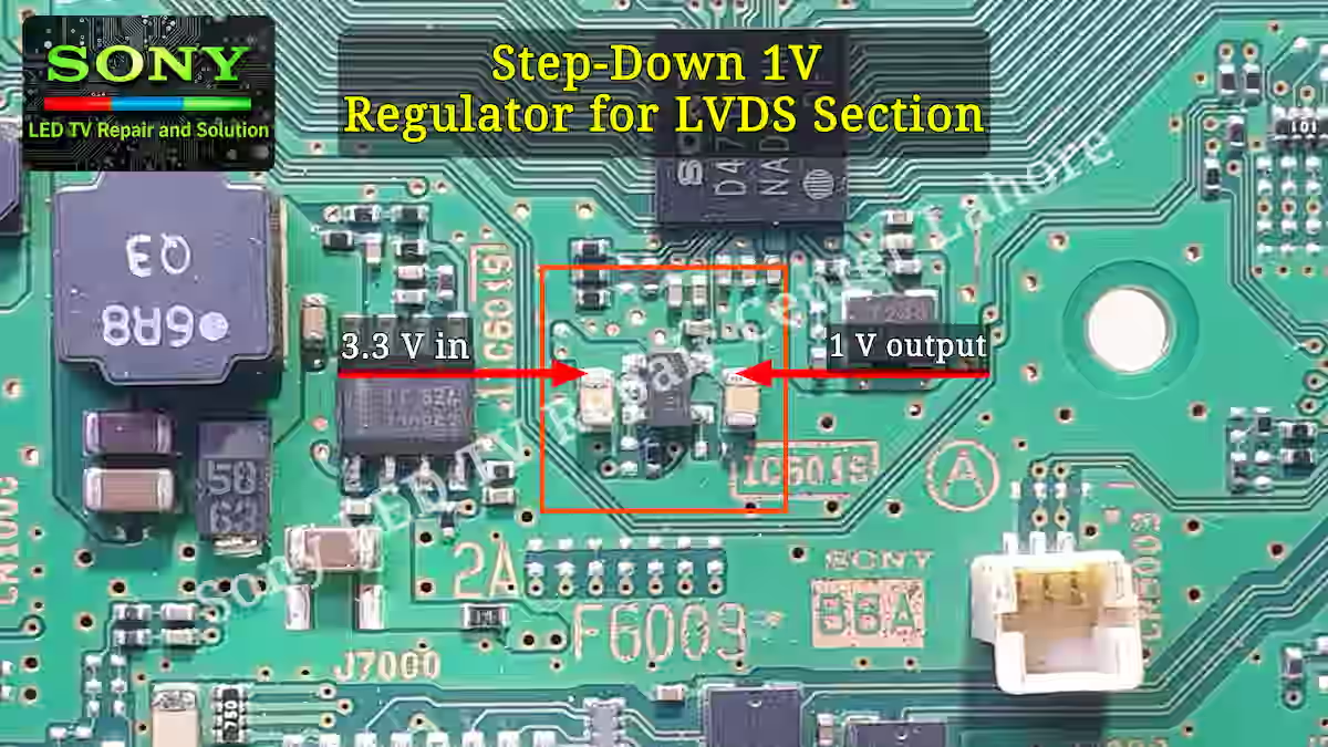
Step-Down 1V Regulator for LVDS Section
In the Sony KLV-40W652D board, this section uses a 5-pin fixed step-down IC to generate the required LVDS supply. It takes a stable 3.3V input from the main power rail and converts it into a precise 1V output for the LVDS IC stage.
The 1V output from this regulator is used directly by the LVDS IC for proper signal processing between the main board and the display panel. This voltage line is very sensitive, and even a small fluctuation can affect display operation, leading to no picture or unstable screen issues.
My Experience with This Section
In my practical experience with this section on the Sony KLV-40W652D board, the enable pin resistor is often found faulty. In several cases, I replaced this resistor and the issue was resolved, so this point should always be checked during troubleshooting.
Another common issue I observed is related to the 3.3V supply IC, which we have already discussed in another article of this same series. When this IC becomes faulty, the step-down section does not receive proper input voltage, which directly affects the 1V generation.
In some cases, the step-down IC itself also gets damaged. I have replaced it multiple times in different boards. However, from experience, it is very important to use a properly rated IC. If a lower current or low-quality IC is used, it may work temporarily but will fail again after some time.
RT9193 IC Pin Connection
In the next section, we will explain the pin configuration of this IC step by step. The details will help in understanding how each pin behaves in the circuit and how the voltage regulation process is controlled in the LVDS section.
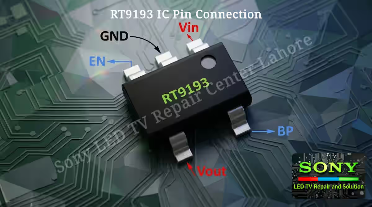
In the image given below, we are showing the layout and circuit connection of this IC. You can clearly observe how it is placed on the board and how it operates within the step-down regulation circuit.
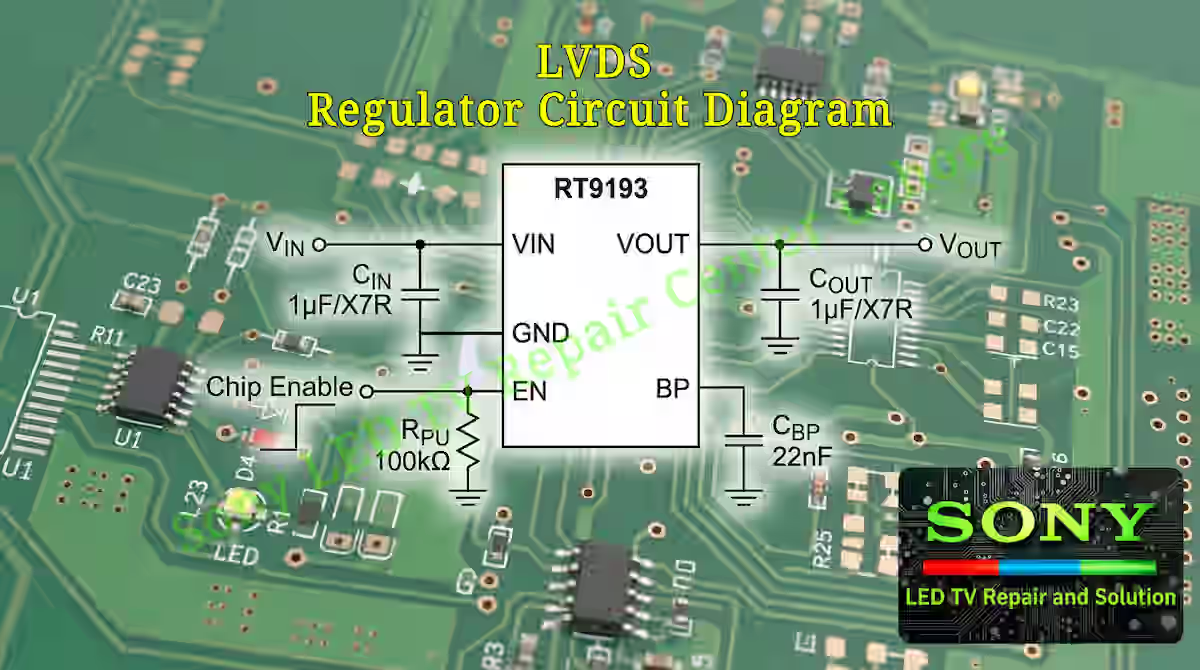
LVDS Regulator Circuit Diagram
In the image given below, you can clearly see the circuit diagram of this step-down voltage regulator section. This diagram helps in understanding how the RT9193 IC is connected with the surrounding components and how the 1V output is generated for the LVDS section in the Sony KLV-40W652D board.
By studying this circuit layout, you can easily understand the working behavior of the IC, including input supply path, enable control, and output regulation stage. It gives a clear practical view of how the voltage is stepped down and delivered to the LVDS IC for proper display operation.
RT9193 IC Pin Description
- Pin 1 (VIN)
This is the main input voltage pin of the IC. It receives the supply voltage from the main power rail, which is then regulated internally by the IC. Proper and stable input voltage on this pin is necessary for correct operation of the regulator. If the input is missing or unstable, the IC will not generate the required output voltage.
- Pin 2 (GND)
This is the ground pin of the IC and acts as the reference point for all internal operations. All input and output voltages are measured with respect to this ground. A weak or broken ground connection can cause unstable operation or complete failure of the regulator output.
- Pin 3 (EN)
This is the enable pin of the IC. When this pin receives a proper high signal, the regulator turns ON and starts producing output voltage. If the enable signal is low or missing, the IC remains in shutdown mode and no output is generated.
- Pin 4 (BP)
This is the bypass pin of the IC. It is normally connected with a capacitor to reduce noise and improve the stability of the internal reference voltage. This helps in providing a clean and stable output. If this pin circuit is disturbed or the capacitor is faulty, the output may become noisy or unstable.
- Pin 5 (VOUT 1V)
This is the main output pin of the IC, which provides a regulated 1V supply. This output is used for the LVDS section and other sensitive low-voltage circuits on the board. If this pin does not produce proper 1V, the LVDS IC will not function correctly, leading to display issues or no picture condition.
Important Advice for Technicians
It is often observed that technicians try to replace this IC with a ready-made regulator module when the original IC gets damaged. This practice is not recommended because these modules usually do not match the exact voltage and current rating required by the circuit.
Using a modified or non-original solution can create serious issues in the long run. It may work temporarily, but it can easily damage the next stage of the circuit or cause repeated failures. Therefore, always avoid circuit modification and try to use the original IC. If the exact part is not available, arrange the correct replacement with proper rating instead of modifying the circuit.
Conclusion
In the Sony Bravia LVDS 1V Voltage Guide, we have clearly understood how the RT9193 IC and its related step-down circuit play a key role in generating a stable 1V supply for the LVDS section in the Sony KLV-40W652D. This voltage line is very critical for proper display communication between the main board and the panel.
From practical repair experience, most faults are related to small components like enable line issues, bypass capacitor problems, or unstable input supply rather than the IC itself. A proper step-by-step checking approach always helps in accurate fault finding without unnecessary replacement. If handled carefully with correct parts, this section can be repaired in a very reliable way in real field conditions.
Related Articles
If you want to go deeper into practical fault finding and step-by-step repair guides from the same Sony Bravia Voltage Description Series for the Sony KLV-40W652D LED TV, you can explore more related write-ups below. These articles are written to help technicians understand real board-level voltage issues in a simple and practical way.
Below you will find links to other detailed guides in this series that cover different voltage sections, IC troubleshooting methods, and common repair cases found in Sony Bravia main boards.
Sony Bravia 5V Power Supply Detail–Read More
Sony Bravia 1.5V Power Supply Fault Guide–Read More
Sony Bravia 1.2V Power Supply Fault Guide–Read More
Sony Bravia 1.8V Power Supply Fault Guide–Read More
KD-49XF8000 2 Blink Error Fix Guide
TPS54332 Circuit Diagram & Pinout

Shaukat Ali has over 30 years of experience in LED TV repair, specializing in chip-level repair work. He is an expert in Sony LED TVs, and also repairs other major brands like Samsung, TCL, Orient, and Haier. His expertise includes display panel faults, motherboard issues, power supply circuits, T-Con, and HDMI faults. Based in Lahore, he shares real-time fault finding cases from daily repair work to help technicians and learners with practical experience.
📞 Contact: +92 321 4066054