
RT6908 IC Programmable Multi Functional Power Solution
In this article RT6908 IC Circuit Diagram & Technical Guide, you will find the complete circuit diagram, block diagram, and detailed pin configuration along with a step-by-step technical explanation of this IC. It is an advanced PMIC solution designed for TFT LCD panels. This IC distributes panel power into multiple DC to DC voltage rails to ensure stable and clean supply for the display section. It also provides proper voltage support to different functional blocks of the TFT panel, which helps in improving overall performance and stability.
RT6908 IC PMIC TFT Panels
This IC is an advanced PMIC (Power Management IC) used in TFT LCD panels to distribute power into different DC to DC voltage rails for various display sections. It provides stable voltage supply to functional blocks such as the gamma section and timing control, which helps improve overall display performance and reduce noise issues. The IC also manages proper power sequencing and regulation to ensure there are no voltage fluctuations during panel startup. Designed for compact and efficient power management, this IC handles multiple voltage outputs smoothly in modern TFT LCD panels, making it an important component for technicians in repair and troubleshooting work.
RT6908 IC Circuit Diagram Overview
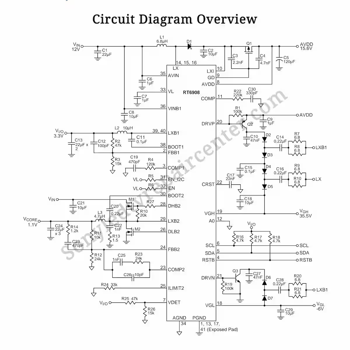
The below RT6908 IC circuit diagram provides a complete view of the power management structure used in TFT LCD panel applications. In this diagram, you can clearly observe the main 12V input supply, along with the regulated VDD 15.6V line that supports different power stages of the panel circuit. The diagram also shows the 3.3V output rail, which is used for logic and control sections, along with the main VIN input voltage path feeding the IC.
In the switching section, the MOSFET operation is clearly illustrated, showing how it controls and regulates power conversion inside the circuit. The diagram further highlights the VCORE voltage line, which plays a key role in internal processing stability, along with the VDET (voltage detect) point, which is used for monitoring and protection purposes. You can also see different feedback resistors and their values, which help maintain accurate voltage regulation throughout the system.
Additionally, the circuit includes important display driving voltages such as VGL and VGH, which are essential for TFT panel gate control operation. The SCL and SDA interface lines are also visible in the diagram, indicating communication control between the IC and other system components. All these elements, including feedback paths and regulation points, work together to maintain stable and efficient panel operation, as clearly shown in the image above.
RT6908 IC Block Diagram
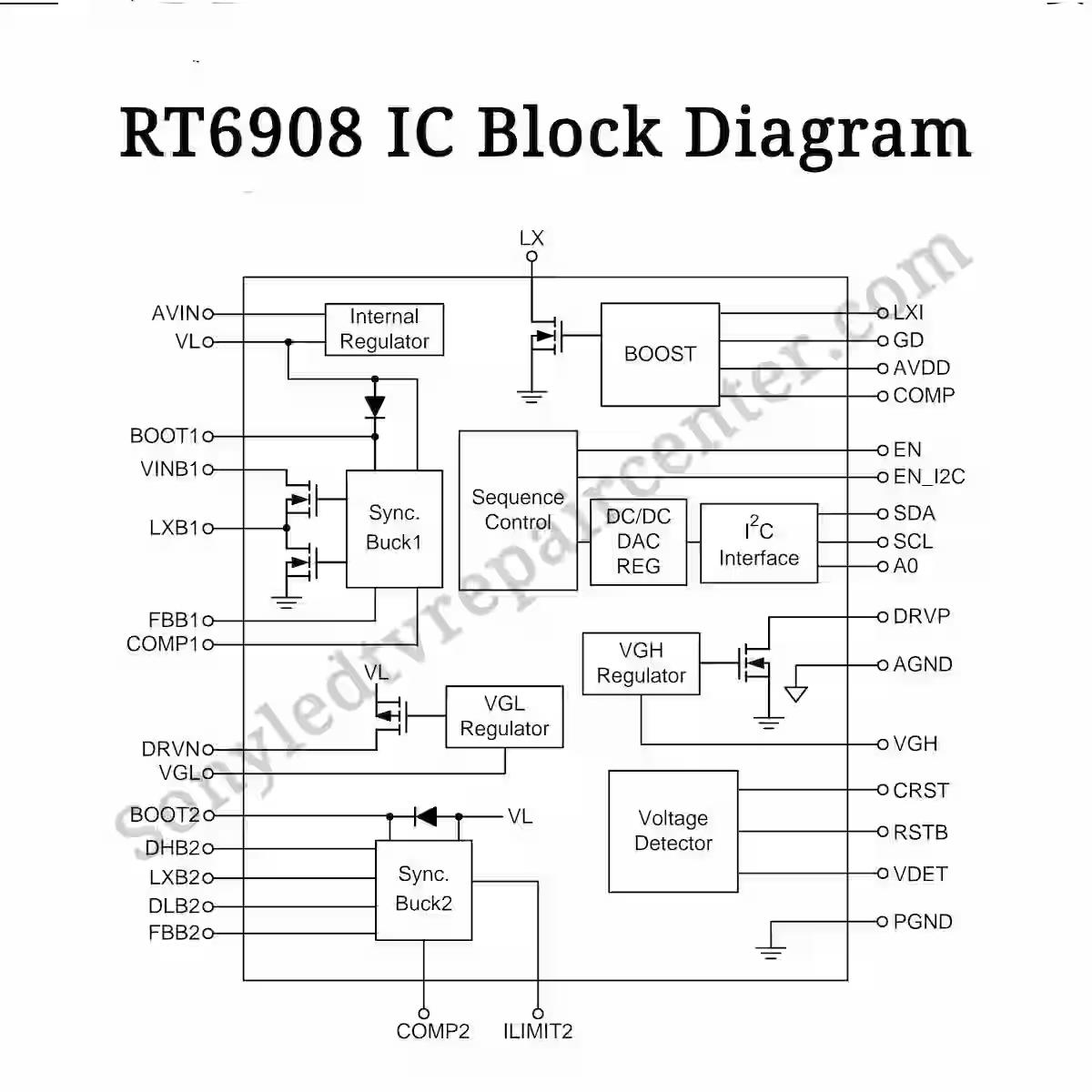
In the below RT6908 IC block diagram, the internal structure of the IC is clearly illustrated, showing how different functional blocks are integrated to manage TFT panel power efficiently. The diagram highlights the boost section, which is responsible for generating higher voltage levels required for panel operation. Along with this, internal regulators are shown that ensure stable and controlled voltage outputs across different stages of the system.
It also includes Sync Block 1, which plays an important role in timing and coordination of internal operations. The sequence control section is clearly visible, managing proper power-up and shutdown order to protect the panel circuitry. In addition, the VDH regulator and VGL regulator are shown, which generate essential display driving voltages for TFT operation. The voltage detector block is also included in the structure, which continuously monitors system voltage levels and helps maintain safe and stable working conditions of the IC.
RT6908 IC PCB Layout Guide
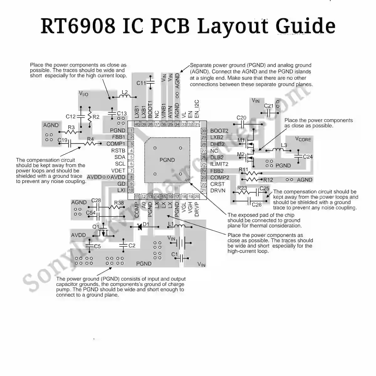
In the below RT6908 IC PCB layout guide, the complete board-level placement of components is clearly shown, making it easier for technicians to understand the real working structure of the circuit. The IC is properly highlighted on the PCB along with all its pin connections, where each pin is labeled with its respective name for easy identification during testing and troubleshooting.
This layout also shows the surrounding SMD components connected to the IC, helping to trace the signal and power paths directly on the board. By following the pin mapping and component placement in this PCB layout, technicians can easily match the schematic with the actual hardware, which greatly simplifies fault finding and repair work in TFT LCD panel circuits.
RT6908 IC Pin Description
Pin 1, 13, 17, 41 (Exposed Pad) – PGND
These pins are power ground (PGND) connections used for the main current return path of the IC. They provide a stable ground reference for high-power switching sections and help reduce noise in the circuit. The exposed pad is also connected to ground and improves heat dissipation and overall stability.
Pin 2 – FBB1
This pin is the feedback input for the boost converter section. It monitors the output voltage through a resistor divider network and helps regulate the voltage level. The IC adjusts the switching operation based on this feedback to maintain a stable output.
Pin 3 – COMP1
This pin is the compensation node for the boost converter control loop. It is used to connect external RC components to stabilize the feedback system. Proper compensation at this pin ensures stable operation and smooth voltage regulation.
Pin 4 – RSTB
This is the reset input pin used to enable or disable the IC operation. When this pin is low, the IC remains in shutdown mode, and when it is high, normal operation starts. It is mainly used for system control and proper startup sequencing.
Pin 5 – SDA
This is the I2C serial data communication pin of the IC. It is used to transfer data between the controller and the IC for configuration and control. Proper pull-up resistance is required for stable communication.
Pin 6 – SCL
This is the I2C serial clock input pin used for synchronization of data communication. It works together with the SDA pin to control data transfer timing between the controller and the IC. A stable clock signal is required for proper and error-free communication.
Pin 7 – VDED
This pin is used for voltage detection input of the IC. It monitors the supply voltage level and ensures proper protection and regulation during operation. Based on this feedback, the IC can enable or disable certain functions to maintain stable working conditions.
Pin 8 – AVDD
This is the analog power supply pin of the IC. It provides a stable voltage to the internal analog circuitry for proper operation. A clean and noise-free supply is required to ensure accurate performance of the internal blocks.
Pin 9 – GD
This is the gate driver output pin of the IC. It is used to drive the external MOSFET by providing switching signals. Proper control from this pin ensures efficient power conversion and stable operation of the boost circuit.
Pin 10 – LX1
This pin is the switching node of the internal boost converter. It is connected to the inductor and external switching components, and handles high-frequency switching operation. It plays a key role in energy transfer and voltage step-up functionality of the circuit.
Pin 11 – COMP
This pin is the compensation node of the control loop. External RC components are connected here to stabilize the feedback system and ensure smooth regulation. Proper compensation helps maintain stable operation and prevents oscillations in the output voltage.
Pin 12 – A0
This pin is used as an address or configuration select input for the IC. It helps define communication or operating settings depending on the system design. Proper logic level at this pin ensures correct IC configuration and operation.
Pin 14, 15, 16 – LX
These pins are the switching nodes of the internal power stage. They are connected to the inductor and handle high-frequency switching current during boost operation. These LX pins play a key role in energy transfer and voltage step-up, ensuring stable power delivery to different output rails.
Pin 18 – VGL
This pin provides the negative gate driving voltage for the TFT panel. It is used to control the turning OFF of the thin film transistors in the display matrix. A stable VGL voltage is important for proper pixel switching and overall display performance.
Pin 19 – VGH
This pin generates the positive gate driving voltage for the TFT panel. It is used to turn ON the thin film transistors in the display matrix. A stable VGH level is essential for proper pixel activation and correct display operation.
Pin 20 – DRVP
This pin is the driver supply output for the gate driver stage of the IC. It provides power to the internal gate driving circuitry to ensure proper switching operation. A stable DRVP voltage is necessary for reliable and efficient control of the external switching components.
Pin 21 – DRVN
This pin is the driver negative supply or return path for the gate driver stage. It works together with DRVP to provide proper biasing for internal switching control circuits. A stable DRVN connection is important for correct gate drive operation and overall circuit stability.
Pin 22 – CRST
This pin is used for chip reset control in the IC. It ensures proper initialization of internal circuits during power-up or fault conditions. When activated, it helps restart the IC operation in a controlled and stable manner.
Pin 23 – COMP2
This pin is the compensation node for the second control loop of the IC. External RC components are connected here to stabilize regulation and improve response of the feedback system. Proper compensation at this pin ensures smooth and stable voltage control without oscillations.
Pin 24 – FBB2
This pin is the feedback input for the second boost or regulation channel of the IC. It monitors the output voltage through a resistor divider network and provides feedback to maintain stable regulation. Based on this signal, the IC adjusts its switching operation to ensure a consistent and accurate output voltage.
Pin 25 – ILIMIT2
This pin is used to set or control the current limit for the second channel of the IC. It helps protect the circuit from overcurrent conditions by restricting excessive current flow. A proper resistor value on this pin ensures safe and stable operation of the power stage.
Pin 26 – DLB2
This pin is used for dynamic load blanking or discharge control in the second channel of the IC. It helps manage transient conditions during switching and improves overall stability of the output. Proper operation of this pin ensures smooth performance under varying load conditions.
Pin 27, 37 – NC
These pins are “No Connection” (NC) pins. They are not internally connected to any functional block of the IC. These pins are left open and should not be used for any external circuit connection.
Pin 28 – DHB2
This pin is used for discharge or high-side blanking control in the second channel of the IC. It helps manage switching transitions and improves stability during load changes. Proper operation of this pin ensures clean and controlled power regulation in the circuit.
Pin 29 – LXB2
This pin is the switching node of the second boost converter channel. It is connected to the inductor and switching components, handling high-frequency switching operation. This pin plays an important role in energy transfer and voltage step-up for the second power stage.
Pin 30 – BOOT2
This pin is the bootstrap supply for the high-side gate driver of the second channel. It provides the necessary floating voltage to drive the high-side MOSFET properly. A bootstrap capacitor is connected between BOOT2 and LXB2 to ensure stable switching operation.
Pin 31 – EN 12C
This pin is the enable control input for the I2C-controlled operation of the IC. It is used to turn the IC ON or OFF through logic control signals. When this pin is activated, the IC starts normal operation under I2C command control.
Pin 32 – EN
This pin is the main enable control input of the IC. It is used to turn the IC ON or OFF depending on the logic level applied. When this pin is enabled, the IC starts normal operation and all regulated outputs become active.
Pin 33 – VL
This pin provides the low-voltage internal supply for the control and logic circuitry of the IC. It ensures stable operation of internal digital blocks and reference circuits. A clean and stable voltage on this pin is necessary for proper IC functionality.
Pin 34 – AGND
This is the analog ground pin of the IC. It is used as the reference ground for internal analog and control circuitry. A clean and low-noise ground connection is important here to ensure stable and accurate operation of the IC.
Pin 35 – AVIN
This pin is the analog input supply of the IC. It provides the main power source for internal analog blocks and reference circuits. A stable and filtered voltage on this pin is essential for proper and noise-free operation of the IC.
Pin 36 – VINB1
This pin is the input supply for the first boost or power conversion stage of the IC. It receives the main DC input voltage that is used for internal switching and regulation. A stable voltage on this pin is necessary for proper boost operation and reliable power conversion.
Pin 38 – BOOT1
This pin is the bootstrap supply for the high-side gate driver of the first channel. It provides the required floating voltage to drive the high-side MOSFET. A bootstrap capacitor is connected between BOOT1 and LX1 to ensure stable and efficient switching operation.
Pin 39 – LXB1
This pin is the switching node of the first boost converter channel. It is connected to the inductor and switching components, handling high-frequency switching signals. This pin plays a key role in energy transfer and voltage step-up for the first power stage of the IC.
Pin 40 – LXB1
This pin is also part of the switching node for the first boost converter channel. It works together with the LX1/LXB1 switching stage to handle high-frequency power switching. This pin helps in stable energy transfer and proper voltage regulation for the first output rail.
Conclusion
In this article RT6908 IC Circuit Diagram & Technical Guide, we have discussed the complete working structure of the IC in a practical technician-focused approach. From the internal block diagram to the circuit behavior and detailed pin description, each section is explained to help understand how this advanced PMIC manages power distribution in TFT LCD panel systems. The IC plays a key role in generating multiple regulated DC to DC voltage rails, ensuring stable operation for different display sections.
Overall, the RT6908 IC is a highly efficient power management solution that integrates boost conversion, regulation, protection, and control functions in a single chip. Its proper understanding is very useful for technicians during fault finding and circuit analysis, especially in modern LCD panel repair work where stable voltage supply is critical for display performance and reliability.
Related Article
For better understanding of related IC circuits and voltage behavior, you can read our other IC technical guides below. These articles will help you improve fault finding skills and understand different power management sections used in LCD/LED TV boards.
MP3398A IC Circuit Diagram – Read More
RT6905 IC Circuit Diagram – Read More
BD28623MUV Audio IC Technical Guide – Read More
Sony KLV-40W652D 3 Blink Error Fix Guide

Shaukat Ali has over 30 years of experience in LED TV repair, specializing in chip-level repair work. He is an expert in Sony LED TVs, and also repairs other major brands like Samsung, TCL, Orient, and Haier. His expertise includes display panel faults, motherboard issues, power supply circuits, T-Con, and HDMI faults. Based in Lahore, he shares real-time fault finding cases from daily repair work to help technicians and learners with practical experience.
📞 Contact: +92 321 4066054